
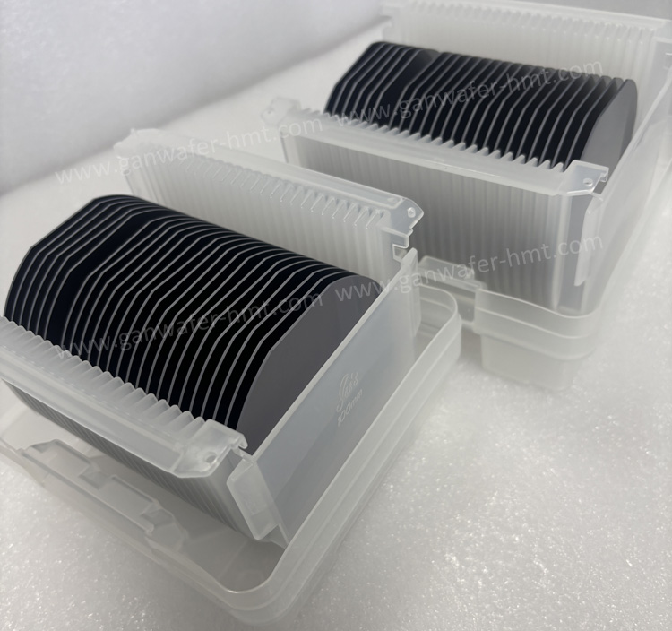
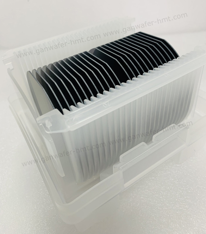
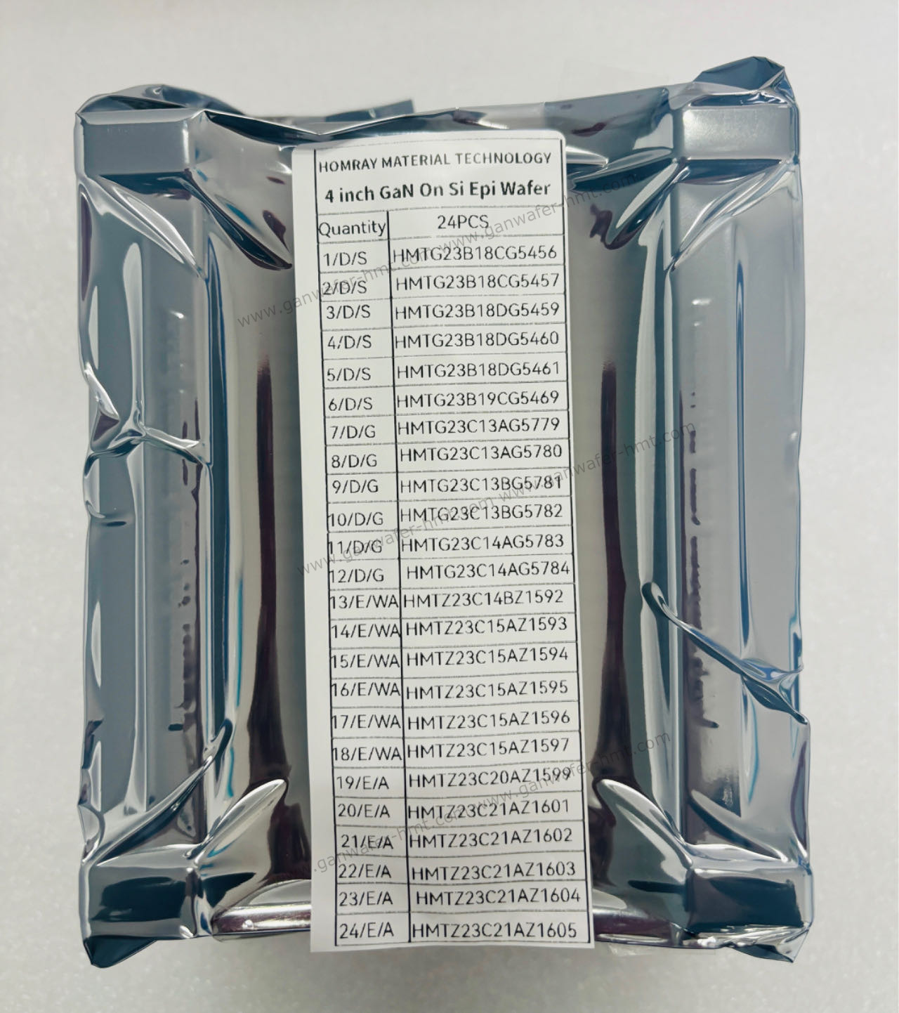
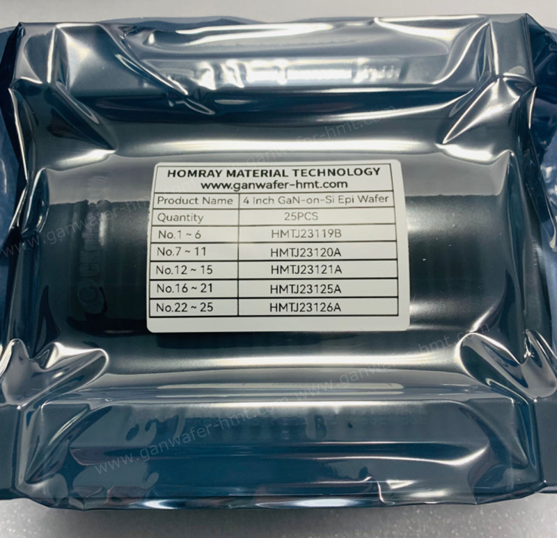
4inch p-GaN/GaN on Si Epitaxial Wafer
Project Description
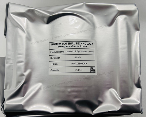
Power Your Next-Generation Devices with HMT's GaN Epitaxial Wafers. As a leading manufacturer, we deliver high-performance p-GaN/GaN-on-Si epi wafers engineered for critical Power HEMT and RF applications. Our technical offerings include:
• Available Diameters: 4-inch, 6-inch, 8-inch
• Structure Options: D-Mode, E-Mode, and RF
Backed by years of epitaxial growth expertise, we are the trusted partner for top semiconductor companies worldwide. Let us ensure the reliability of your most advanced designs—contact us for a consultation.
![]() E-mail: kim@homray-material.com;tina@homray-material.com
E-mail: kim@homray-material.com;tina@homray-material.com
HMT Silicon Carbide (SiC) Wafer Website: www.sicwafer-hmt.com