
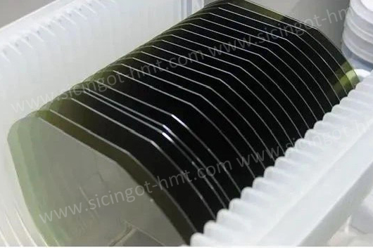
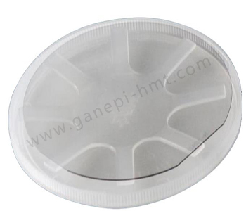
Third-generation semiconductor materials—SiC and GaN —are now in the spotlight. HMT company supply both GaN-on-Si and GaN-on-SiC Epi Wafer including 4inch 6inch and 8inch to all over the world. Thanks to their higher voltage tolerance, lower energy consumption, and superior thermal performance, they are considered the core materials for next-generation power and RF devices.
First, What Are Third-Generation Semiconductors?
Semiconductor materials are broadly categorized into three generations based on their bandgap:
First Generation: Silicon (Si) and germanium (Ge), dominating traditional ICs, microprocessors, and circuits.
Second Generation:Gallium arsenide (GaAs) and indium phosphide (InP), mainly used in RF and optical communications.
Third Generation:Silicon carbide (SiC) and gallium nitride (GaN), which are wide-bandgap semiconductors.
Compared to silicon, SiC and GaN offer larger bandgaps, higher breakdown voltages, faster switching speeds, and lower on-resistance, making them ideal for high-frequency, high-voltage, and high-temperature environments. They are the perfect materials for power electronics and RF communications.
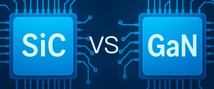
SiC vs. GaN
1. Performance
SiliconCarbide (SiC):
- Breakdown electric field strength: 2.8 MV/cm, suitable for high-voltage applications above 1200V.
- High thermal conductivity and excellent high-temperature resistance.
- However, substrate growth requires 2700°C high-temperature processes, leading to higher costs.
GalliumNitride (GaN)
- Breakdown electric field strength: 3.3 MV/cm, switching frequencies can reach MHz levels, with lower power losses.
- Baliga Figure of Merit (BFOM) is nearly twice that of SiC, but thermal conductivity is lower, requiring optimized heat dissipation designs.
2. Cost
SiC substrates are expensive, but their TO-247 packaging (compatible with silicon-based systems) enables rapid replacement of traditional IGBTs.
GaN reduces costs by using silicon-based substrates, and **8-inch wafer production** has cut per-device costs by 30%.
SiC is expanding 8-inch wafer production, while GaN is advancing vertical structures and monolithic integration to break the 1200V voltage barrier.
3. Applications
SiC: Mainly used in EV traction inverters, industrial power supplies, PV inverters, and power grid transmission systems.
GaN: Primarily deployed in consumer electronics, 5G RF power amplifiers, radar systems, and high-frequency communications.
4. Market Landscape
- The global SiC power device market was worth $2 billion in 2023 and is projected to reach $6.5 billion by 2028, with a CAGR exceeding 25%.
- The GaN power device market was valued at $370 million in 2023 and is expected to grow to $2 billion by 2028, driven by strong demand in consumer electronics and communications.
This fierce competition between SiC and GaN will shape the future of power and RF electronics. Who will ultimately reign supreme? The battle is on!
![]() M.P: +86-15366208370 ; +86-15366203573
M.P: +86-15366208370 ; +86-15366203573
![]() E-mail: kim@homray-material.com;tina@homray-material.com
E-mail: kim@homray-material.com;tina@homray-material.com
HMT Silicon Carbide (SiC) Wafer Website: www.sicwafer-hmt.com