
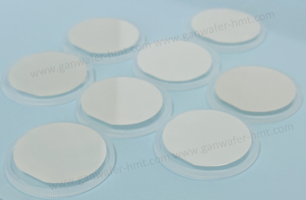
Un-doped/Si-doped GaN Substrate
Project Description
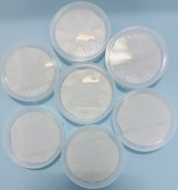
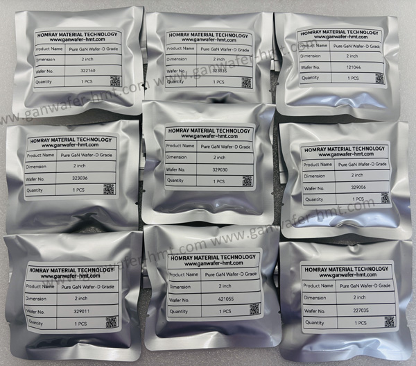
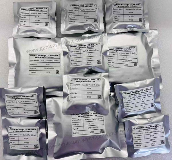
HMT is a leading manufacturer of 2inch and 4 inch free-standing GaN substrate wafers, delivering high-quality products at highly competitive prices. We meet diverse application needs with our standard Un-doped / Si-doped N-type, available in 400um/450μm thickness with DSP or SSP finishes. We are also driving industry advancement with our new large-format 6-inch and 8-inch GaN substrates. As your strategic partner in innovation, we provide the foundational materials for next-generation devices. Contact our team today for inquiries.
![]() E-mail: kim@homray-material.com;tina@homray-material.com
E-mail: kim@homray-material.com;tina@homray-material.com
HMT Silicon Carbide (SiC) Wafer Website: www.sicwafer-hmt.com