
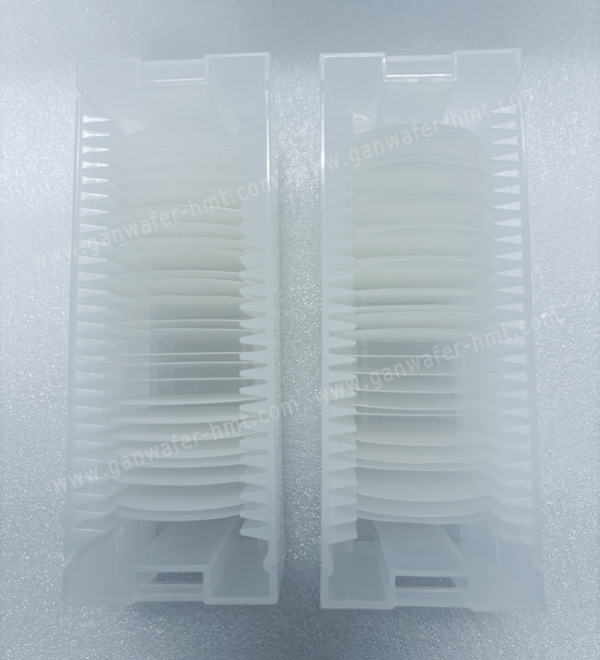
2 inch Si-doped GaN on Sapphire Wafer
Dimensions: 50.8± 0.5 mm
GaN Thickness:4.5µm
Sapphire Thickness:
Useable Surface Area:> 90%
Product Description
HMT provides high-quality 2 inch Si-doped GaN on Sapphire Wafer designed for advanced semiconductor applications including optoelectronics, RF devices, and high-performance electronic components. As a professional GaN on Sapphire Wafer manufacturers, we specialize in supplying GaN epitaxial wafers with excellent crystal quality, uniform thickness, and reliable electrical performance.
Silicon-doped gallium nitride (Si-doped GaN) is an n-type semiconductor material that offers outstanding properties such as wide bandgap, high electron mobility, high breakdown voltage, and excellent thermal stability. By growing GaN epitaxial layers on sapphire substrates, these wafers provide a cost-effective and scalable solution for next-generation semiconductor device manufacturing.
Our 2 inch GaN on Sapphire wafers are widely used by research institutions, LED manufacturers, and semiconductor companies for device development and mass production.
Product Features
High-Quality GaN Epitaxial Layer
The GaN layer is grown on a sapphire substrate using advanced epitaxial growth technology to achieve stable crystal structure and consistent wafer performance.
Si-Doped N-Type Conductivity
Silicon doping provides controlled electrical properties, making the wafers suitable for electronic and optoelectronic device fabrication.
Excellent Material Properties
- Wide bandgap semiconductor material
- High electron mobility
- High thermal conductivity
Reliable Wafer Performance
Our GaN on Sapphire wafers feature:
- Uniform GaN thickness
- Low defect density
- Good surface morphology
Technical Specifications
| Parameters | Specifications |
| Product | 2 Inch Si-doped GaN on Sapphire Wafer |
| Substrate Material | Sapphire (Al₂O₃) |
| Wafer Diameter | 2 inch |
| Semiconductor Material | Gallium Nitride (GaN) |
| Conductivity Type | N-type |
| Dopant | Silicon (Si) |
| GaN Layer Thickness | 4.5±0.5um |
| Surface | Ga-face |
| Surface Finish | Epi-ready |
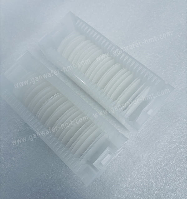
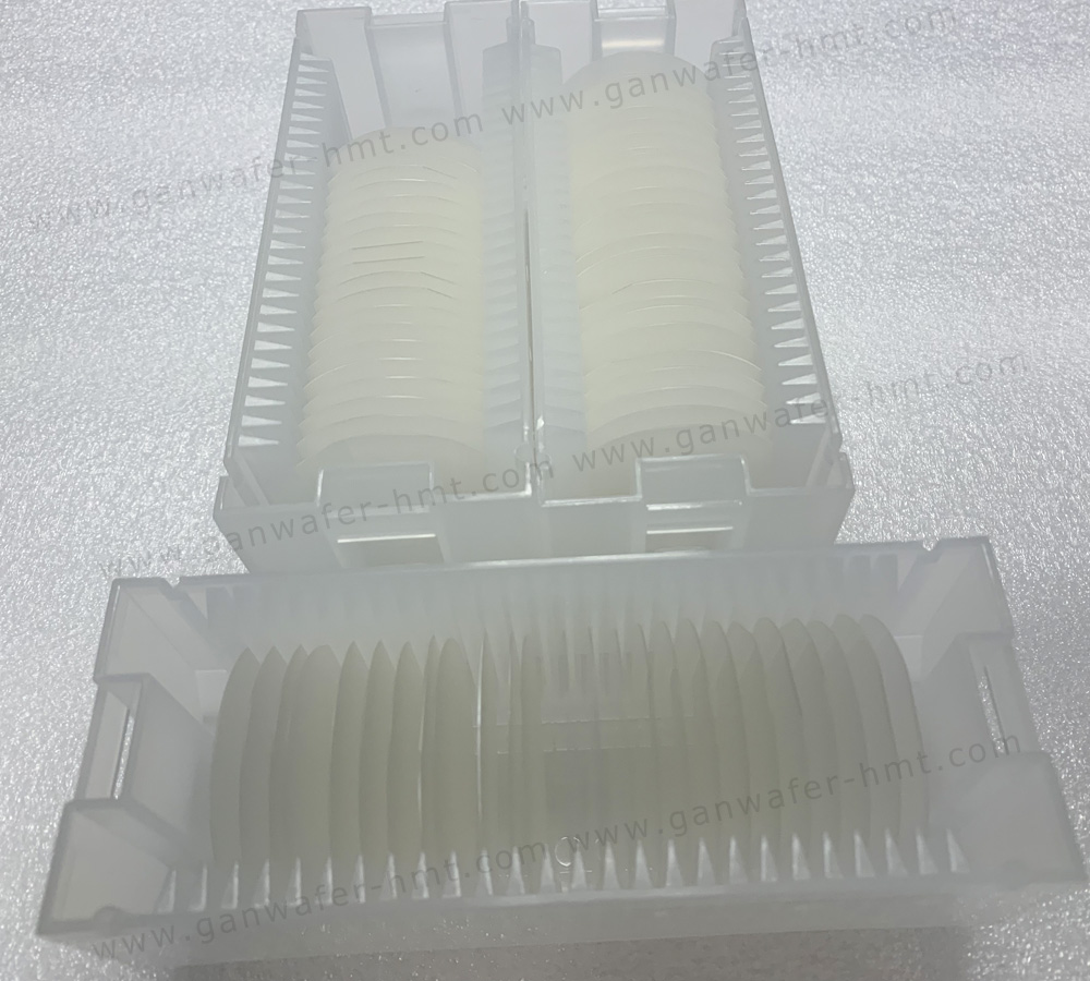
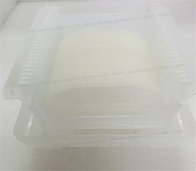
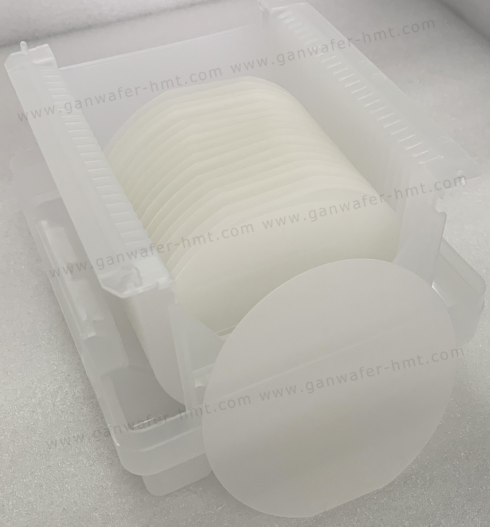
| Package | 25PCS in one Cassette |
Why Choose HMT as Your GaN on Sapphire Wafer Manufacturer?
HMT is a trusted supplier of advanced semiconductor materials, offering reliable GaN on Sapphire Wafer manufacturing solutions for global customers.
Our advantages include:
a. Professional GaN wafer manufacturing capability
b. High-quality epitaxial wafer production
c. Customized wafer specifications
d. Strict quality control system
e. Support for research and industrial applications
f. Reliable global semiconductor material supply
We are committed to providing high-performance 2 inch Si-doped GaN on Sapphire wafers to meet the requirements of emerging semiconductor technologies.
FAQ
What is GaN on Sapphire Wafer?
GaN on Sapphire Wafer is a semiconductor wafer consisting of a gallium nitride epitaxial layer grown on a sapphire substrate. It combines GaN's excellent electronic properties with sapphire's cost efficiency and availability.
Why use sapphire as a GaN substrate?
Sapphire substrates offer good thermal stability, mechanical strength, and lower cost compared with some alternative substrates, making them widely used for GaN-based LEDs and semiconductor devices.
Related Products

 E-mail: kim@homray-material.com;tina@homray-material.com
HMT Silicon Carbide (SiC) Wafer Website: www.sicwafer-hmt.com