
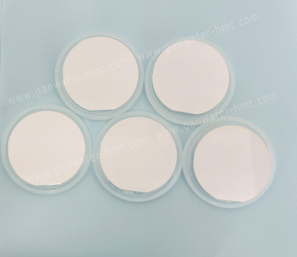
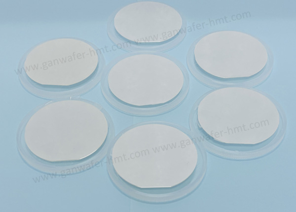
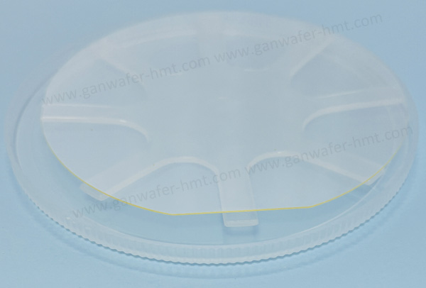
2 Inch SSP Freestanding GaN Substrate for GaN Epitaxy
Dimensions: Ф 50.8 mm ± 0.5 mm
Thickness:400 ± 25 µm
Useable Surface Area: > 90%
Grade: D R P
Product Description
2 Inch SSP Freestanding GaN Substrate for GaN Epitaxy Applications
HMT provides 2 inch SSP freestanding GaN substrates designed as a high-quality native platform for GaN epitaxial growth and advanced semiconductor device development. Unlike conventional GaN layers deposited on foreign substrates, a freestanding GaN substrate provides a bulk gallium nitride crystal surface that enables improved lattice compatibility and a more suitable foundation for homoepitaxial GaN device fabrication.
The Single Side Polished (SSP) surface of this GaN substrate is optimized for epitaxial processes, offering excellent surface uniformity and improved control during subsequent device manufacturing steps. HMT's 2 inch SSP GaN substrates are suitable for researchers, semiconductor manufacturers, and device developers working on high-performance GaN electronics, RF components, optoelectronic devices, and next-generation power semiconductor technologies.
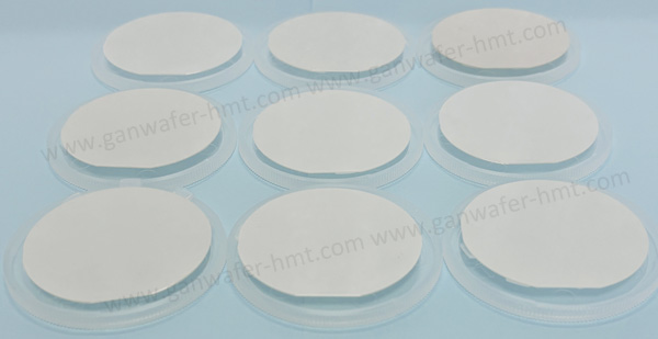
SSP Surface Designed for High Quality Epitaxial Growth
The surface condition of a substrate plays an important role in determining epitaxial layer quality.
Our SSP freestanding GaN substrates provide:
a. Smooth polished growth surface
b. Improved surface uniformity
c. Reduced interface defects
d. Reliable epitaxial process compatibility
These characteristics make them suitable for GaN homoepitaxy and advanced semiconductor device research.
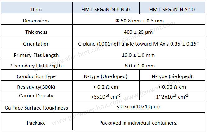
Advantages of Native Freestanding GaN Substrate
Better Crystal Matching
Since the substrate material and epitaxial layer are both GaN, freestanding GaN provides superior crystal compatibility compared with hetero-substrate solutions.
Benefits include:
- Reduced lattice mismatch
- Lower defect generation
- Improved device performance potential
High Thermal Performance
GaN materials offer excellent thermal stability and wide bandgap characteristics.
Freestanding GaN substrates are suitable for devices requiring:
- High power operation
- High frequency switching
- High temperature reliability

What is an SSP freestanding GaN substrate?
An SSP freestanding GaN substrate is a bulk GaN crystal wafer with one polished surface designed for epitaxial growth and semiconductor fabrication.
Why use freestanding GaN instead of GaN-on-Sapphire?
Freestanding GaN provides a native GaN crystal platform, which can reduce lattice-related defects and improve epitaxial layer quality.
Related Products


 E-mail: kim@homray-material.com;tina@homray-material.com
HMT Silicon Carbide (SiC) Wafer Website: www.sicwafer-hmt.com