
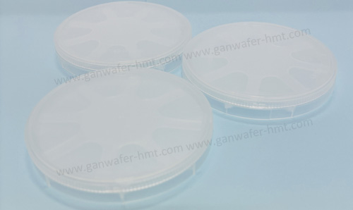
4 Inch Si-doped Freestanding GaN Wafer
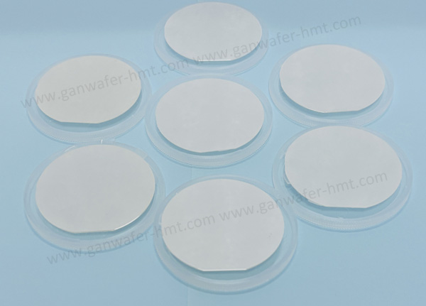
Dimensions: Ф 100 mm ± 0.3 mm
Thickness: 450 ± 30 µm
Useable Surface Area: > 90%
Grade: D R P
Product Description
4 Inch Si-doped Freestanding GaN Wafer with Double Side Polished Surface
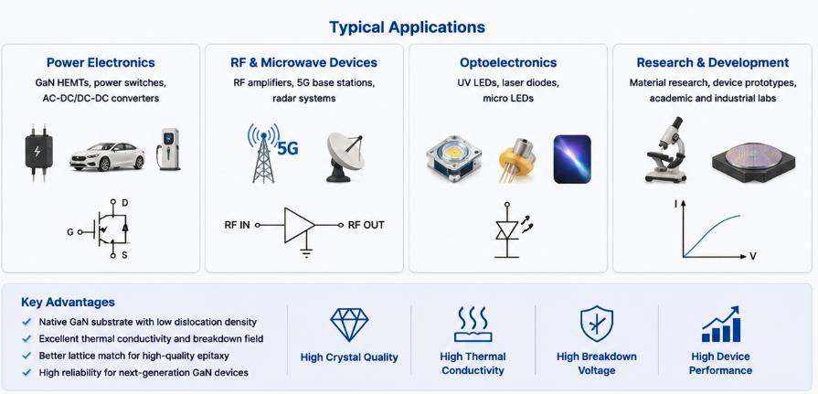
HMT provides 4 inch Si-doped freestanding GaN wafers developed for advanced GaN semiconductor device fabrication, including power electronics, RF components, and optoelectronic applications.
Unlike GaN films grown on foreign substrates, a freestanding GaN wafer is a native gallium nitride crystal substrate that provides an ideal foundation for high-performance GaN devices. The absence of a lattice-mismatched support substrate helps improve crystal quality, thermal stability, and device reliability.
The Si-doped GaN wafer supplied by HMT features controlled n-type conductivity, excellent crystal uniformity, and a double side polished (DSP) surface suitable for demanding epitaxial and semiconductor processing requirements.
In addition to Si-doped GaN wafers, HMT also provides Un-doped GaN wafers and Fe-doped GaN wafers to meet different electrical performance requirements, including high-resistivity applications, RF devices, and advanced GaN research. Our 4 inch (100mm) freestanding GaN substrates are available with customized thickness, carrier concentration, resistivity, and surface specifications.
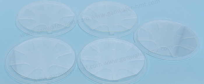
Doping Options for 4 Inch Freestanding GaN Wafers
HMT offers different doping configurations according to application requirements.
Si-doped GaN Wafer
Si-doped GaN wafers provide controlled n-type conductivity and are widely used for electronic device applications.
Advantages: Adjustable carrier concentration/ Low electrical resistance / Suitable for power device structures / Compatible with GaN epitaxial processes
Typical applications: GaN power transistors/ Vertical GaN devices / High-frequency semiconductor devices
Un-doped GaN Wafer
Un-doped GaN wafers provide intrinsic GaN material characteristics with high purity and excellent crystal quality.
Advantages: High material purity / Low background carrier concentration / Suitable for fundamental research and advanced device development
Applications: GaN material research / Epitaxial development / Experimental semiconductor structures
Fe-doped GaN Wafer
Fe-doped GaN wafers are designed for high-resistivity semiconductor applications.
Advantages: High resistivity control / Reduced parasitic electrical effects / Suitable for RF and high-frequency devices
Applications: RF GaN devices /Microwave electronics / High-frequency semiconductor components

FAQ
What is a Si-doped GaN wafer?
A Si-doped GaN wafer is a gallium nitride substrate with silicon doping introduced to control electrical conductivity, commonly used for GaN electronic device fabrication.
What surface finish is available for this GaN wafer?
HMT provides double side polished (DSP) freestanding GaN wafers with customized surface specifications.
Related Products

 E-mail: kim@homray-material.com;tina@homray-material.com
HMT Silicon Carbide (SiC) Wafer Website: www.sicwafer-hmt.com