
GaN On Si Epi Wafer Power HEMT Manufacturer
GaN-On-Si Epi Wafer For Power HEMT-D Mode
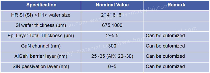
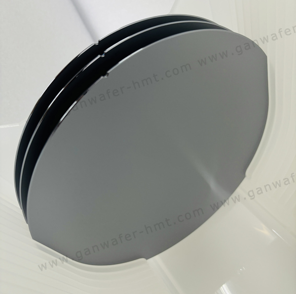
Substrate Diameter: 4-8 inch(111)
Substrate Thickness: 675,1000um
Epi Layer Total Thickness: 2~5.5um
Product Description
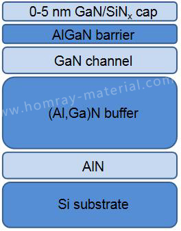
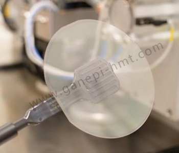
As the leading manufacturer and supplier of GaN (Gallium Nitride) Epi (Epitaxial) wafer and GaN-On-Si Epi Wafer For Power HEMT application. Homray Material Technology offers 2inch 4inch 6inch and 8inch GaN ) on Si Epi wafer for power switching. The HMT650V product is a state-of-the-art (Al,Ga)N/GaN heteroepitaxial layer structure deposited crack-free on a (111) Si-wafer for high voltage power switching applications. Homray Material Technology offers two standard HEMT structures: one having an Al0.25Ga0.75N barrier w/o an AlN spacer layer and the other having an Al0.25Ga0.75N barrier with an AlN spacer layer. Custom barrier, cap layer and in-situ SiN designs are available upon request.
The epitaxial layer consists of an active heterostructure based on an AlGaN layer and a GaN channel, providing high electron mobility and low sheet resistivity.The proprietary high-voltage buffer design offers low leakage currents, high breakdown voltage, low dispersion and a consistently low wafer bow.
Standard Layer Specifications For Power HEMT-D MODE
Please contact us for GaN-on-Si Power HEMT-E MODE detailed structure.
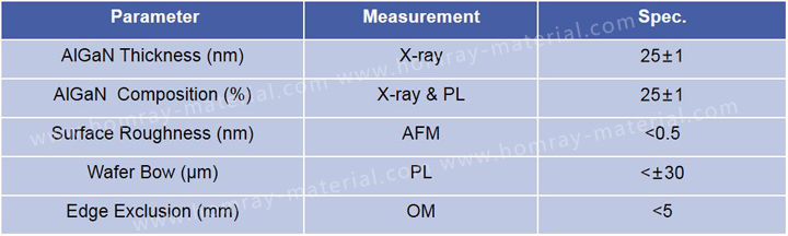
Characterization Specifications
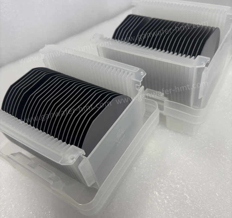
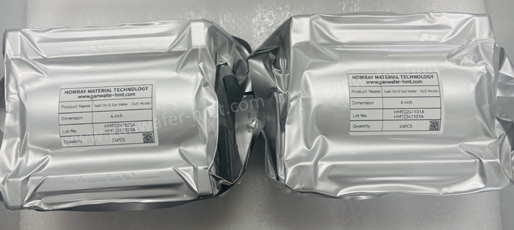
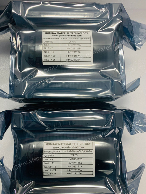
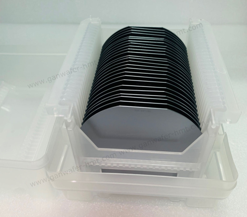
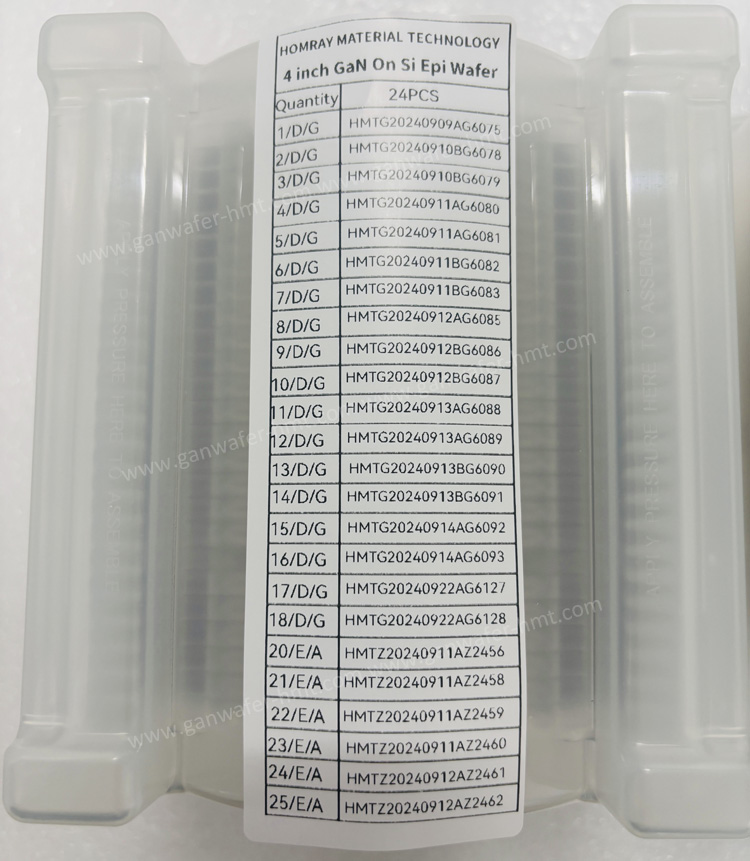
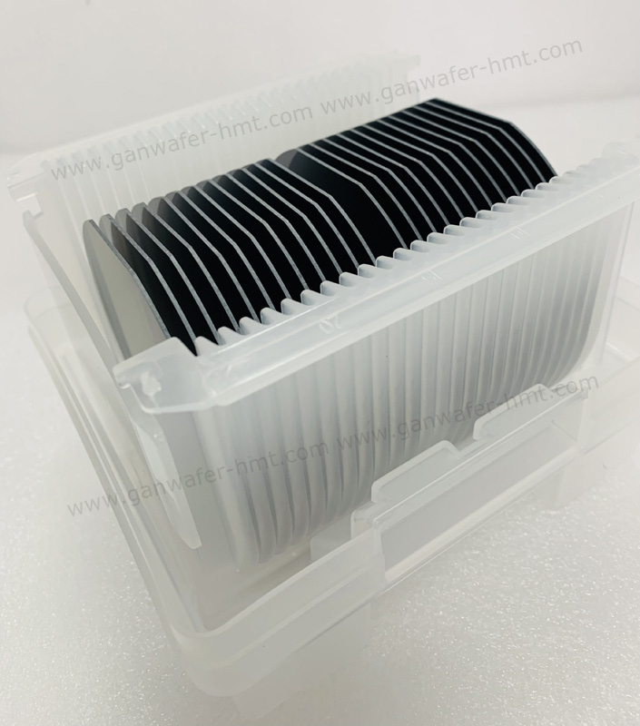
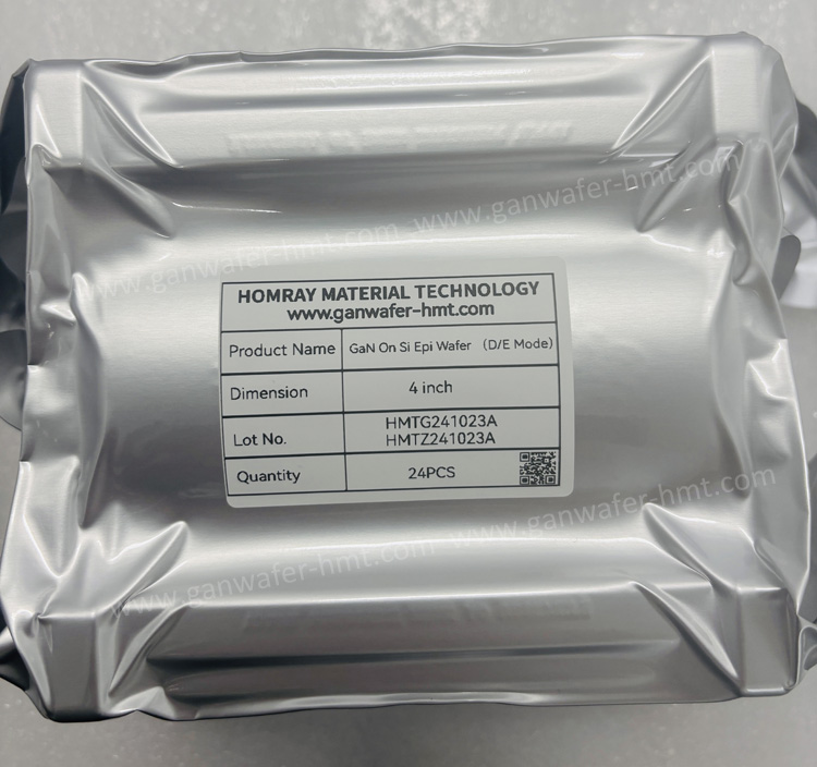
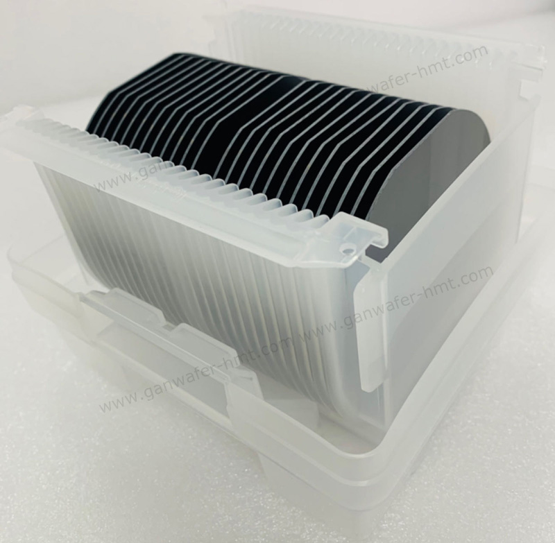
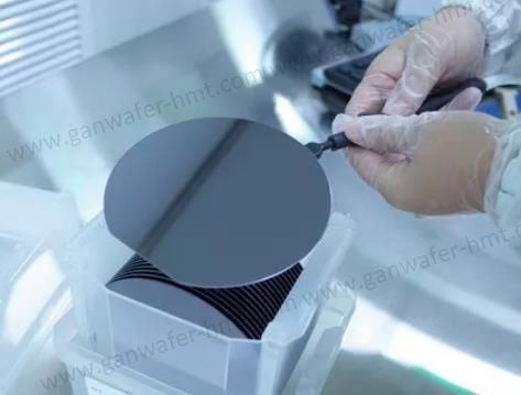
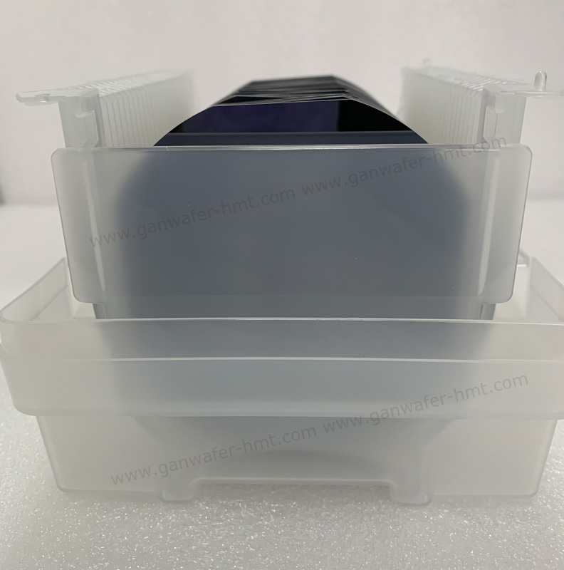
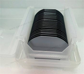
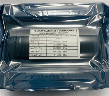
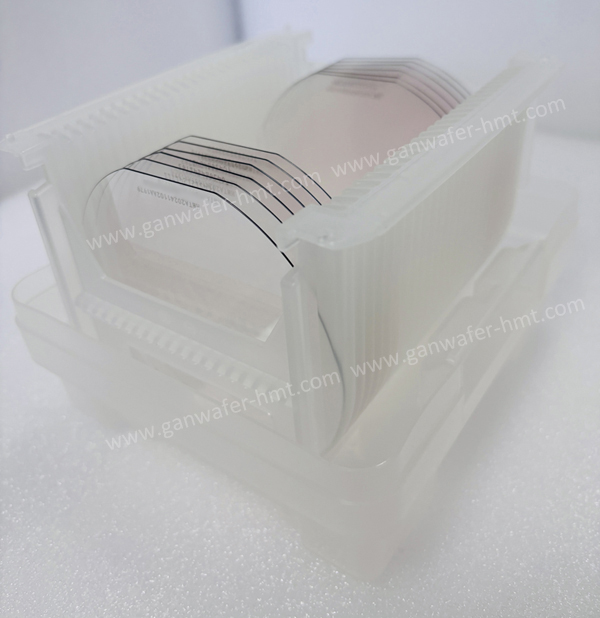
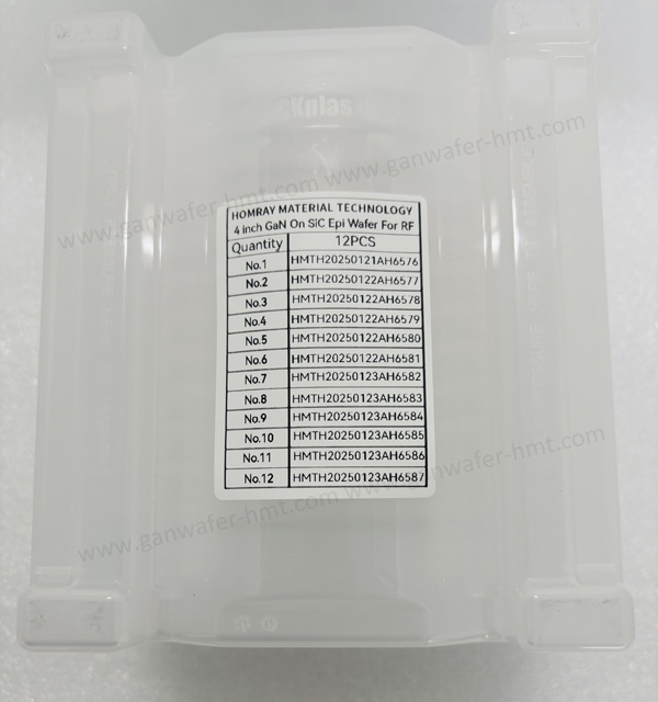
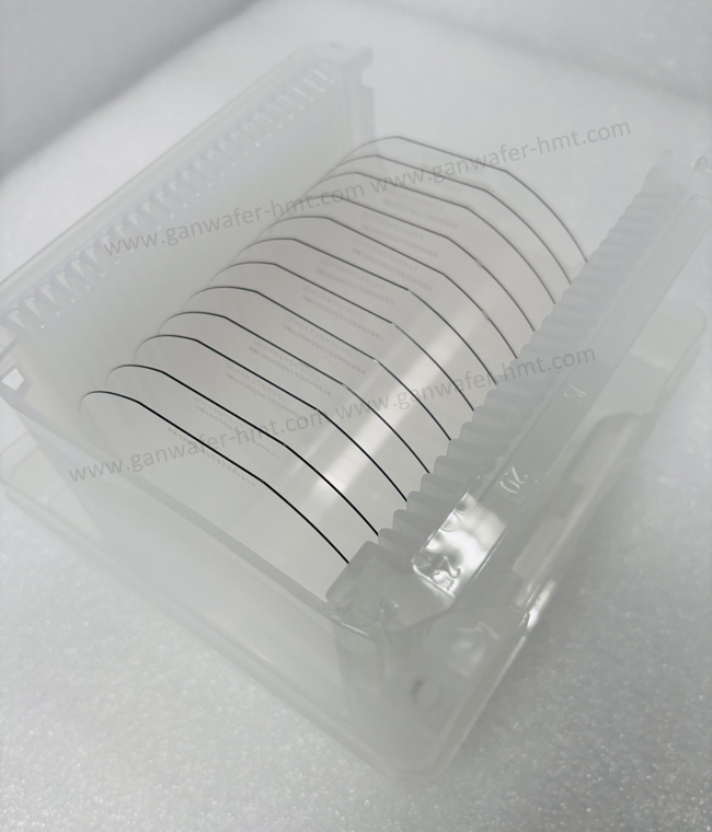
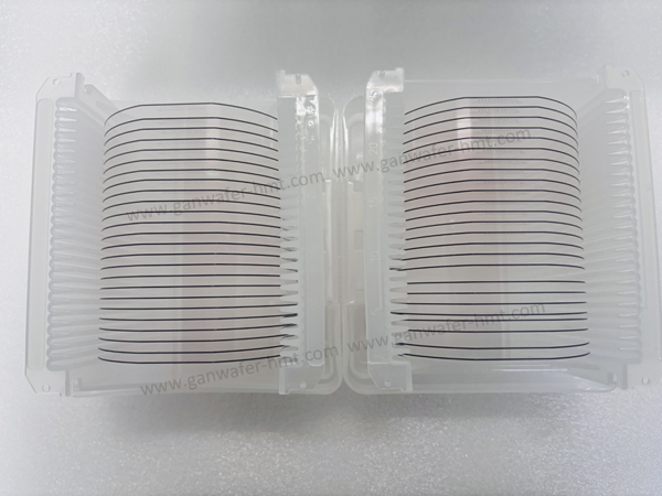
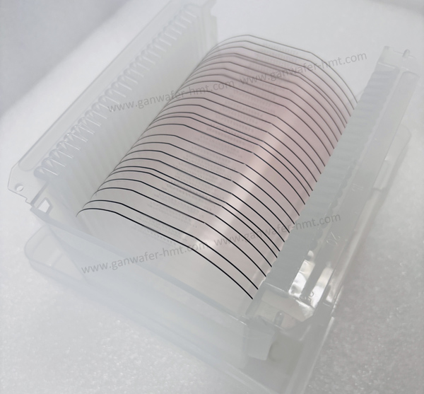
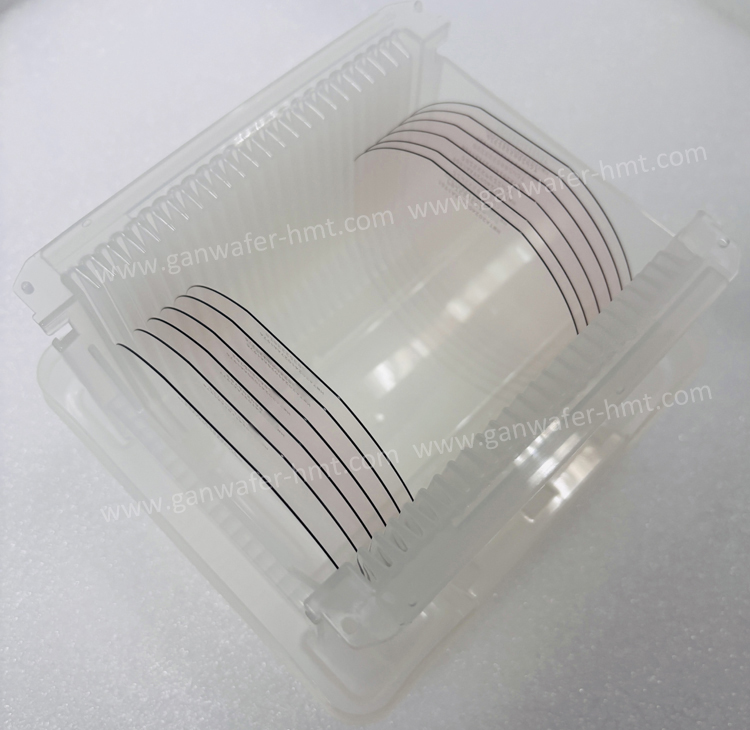
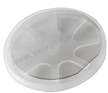
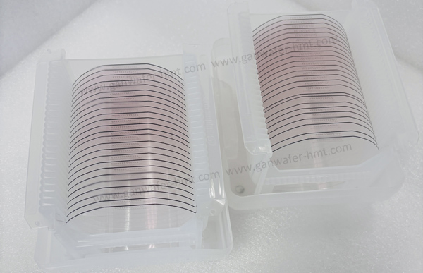
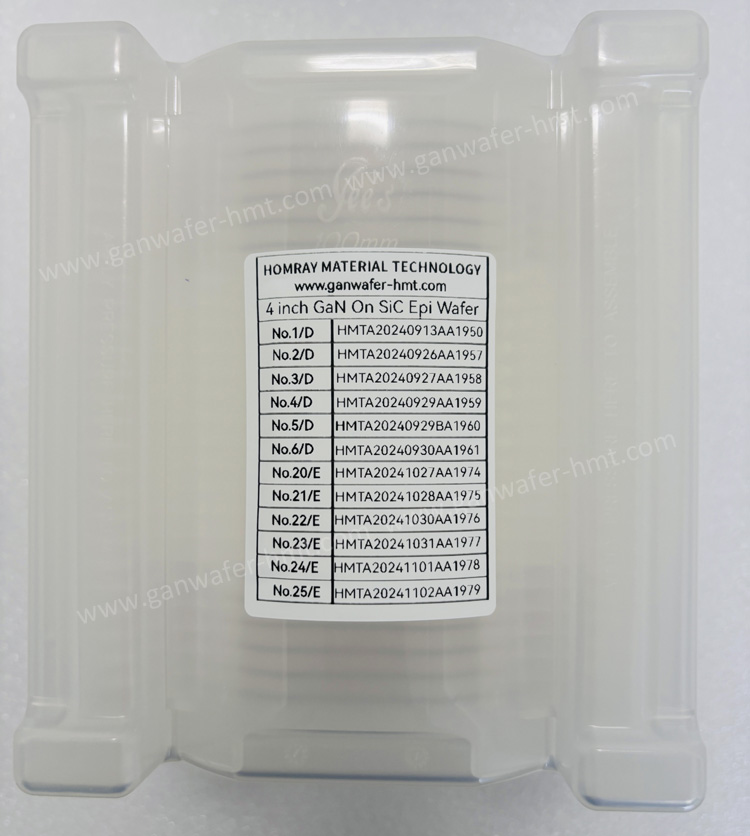
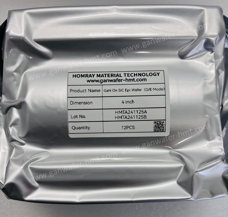
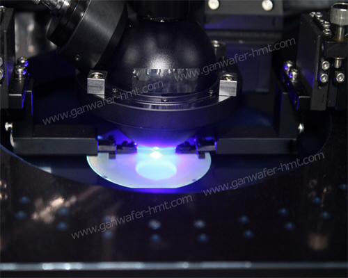
Standard Layer Structure For D mode GaN Epi Wafer Package Picture
Related Products
![]() E-mail: kim@homray-material.com;tina@homray-material.com
E-mail: kim@homray-material.com;tina@homray-material.com
HMT Silicon Carbide (SiC) Wafer Website: www.sicwafer-hmt.com