
D-HEMT AlGaN/GaN On Si Epi Wafer Supplier
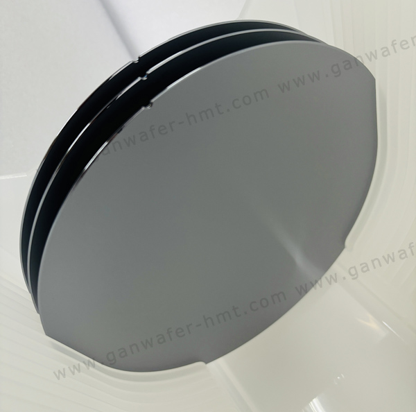
GaN-On-Si Epi Wafer
Substrate Size: 4/6/8 inch
Substrate Thickness: 675um 1000um
GaN Buffer Layer: 2-3um
Product Description
Find GaN Epi Grown on Si Substrate manufacturer and supplier from pfofessional HMT company. Cutstomized 4inch to 8inch D-HEMT GaN-on-Si Epi Wafer structure and parameters are available in HMT. We have both SiN protection layer and GaN protection layer for D-mode GaN/Si Epi wafer.
Epitaxy refers to the method of depositing a monocrystalline film on a monocrystalline substrate. Homoepitaxy is a kind of epitaxy performed with only one material. This technology is applied to growing a more purified film than the substrate and fabricating layers with different doping levels. Heteroepitaxy is a kind of epitaxy performed with materials that are different from each other. Examples include GaN on Sapphire or GaN on SiC etc.
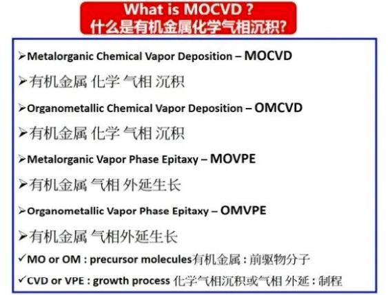
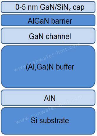
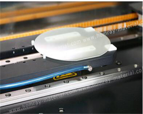
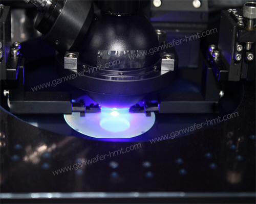
What is MOCVD? HMT GaN on Si Structure
Application of GaN Epi Wafer
Permanent magnet motor refers to a kind of electromagnetic device based on the Faraday law of electromagnetic induction to achieve electric energy conversion or transfer. The main role is to generate driving torque, as the power source of electrical appliances or various machinery. Motors are widely used in consumer electronics, household appliances, industrial manufacturing, robotic and other fields.
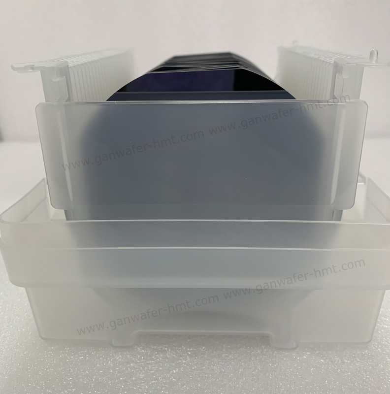
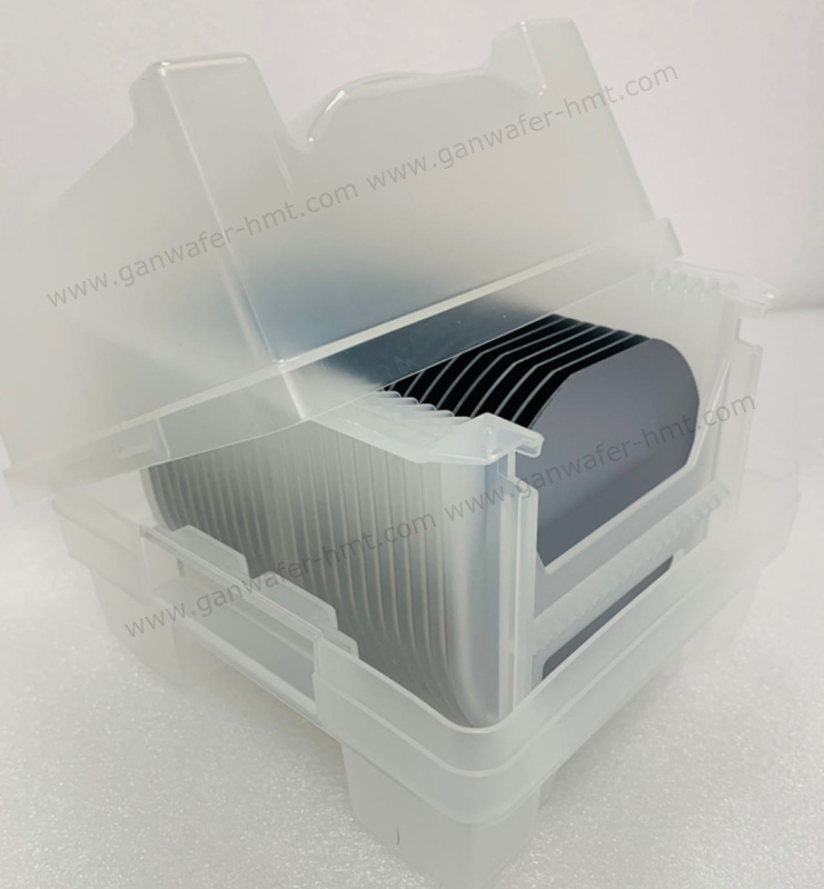
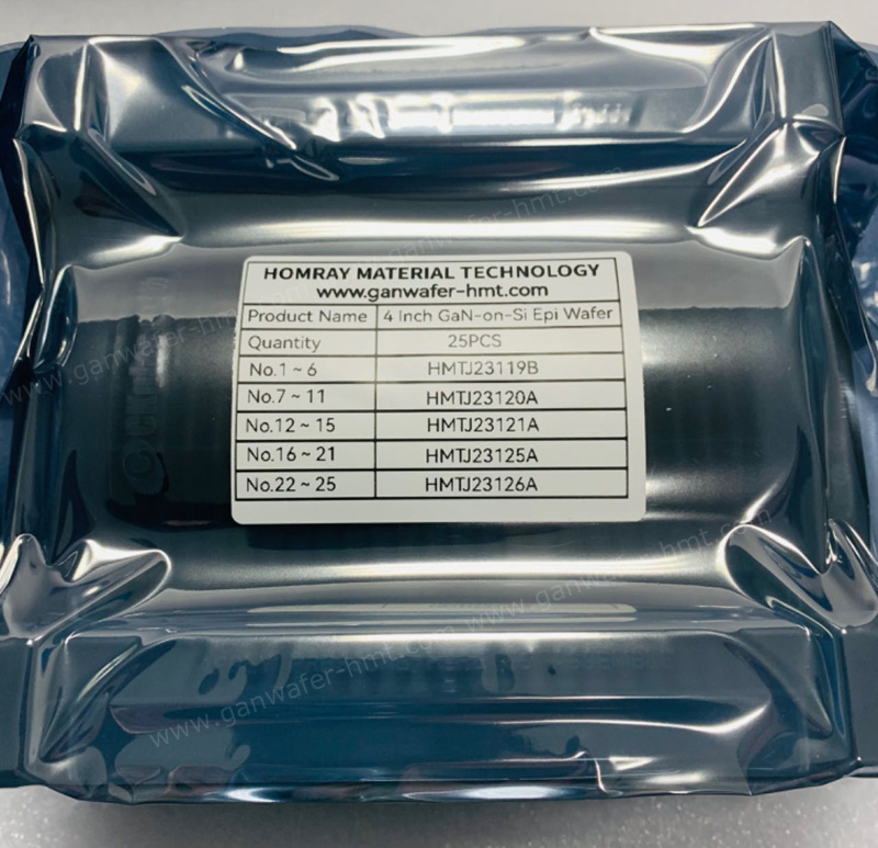
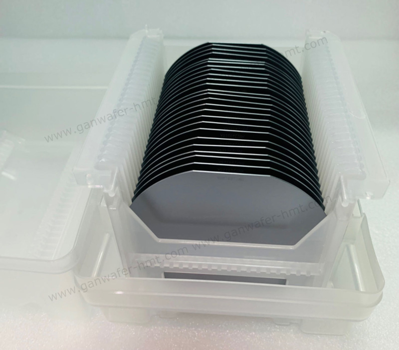
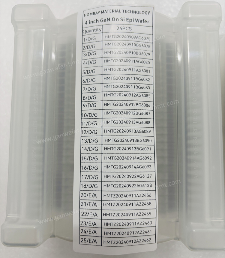
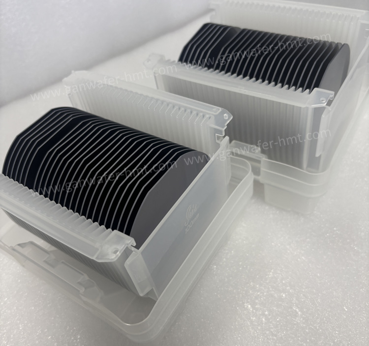
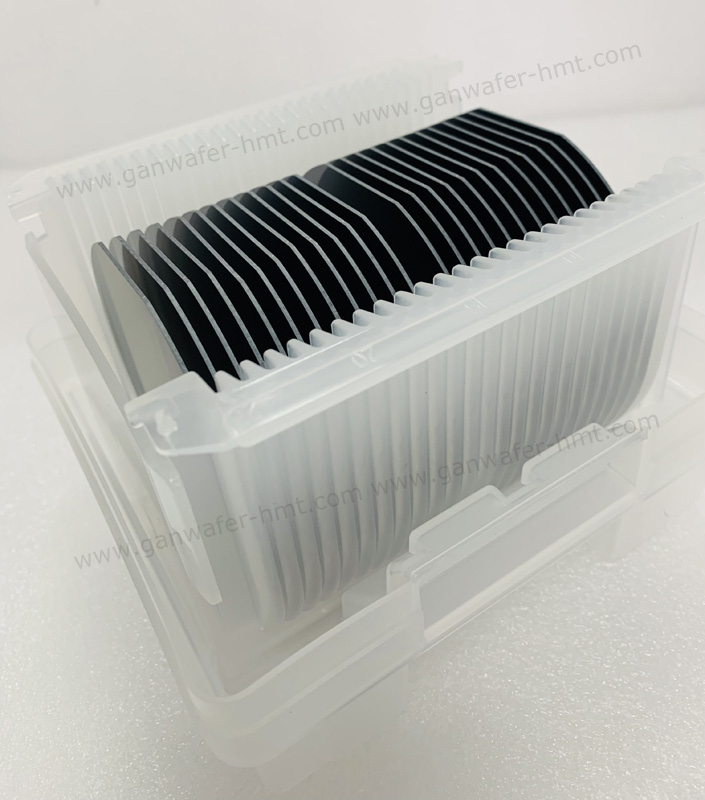
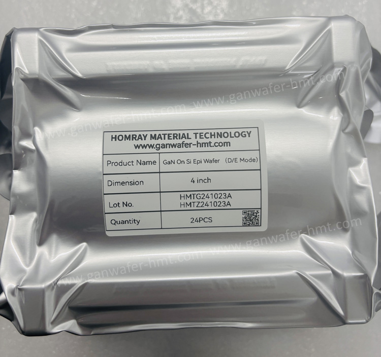
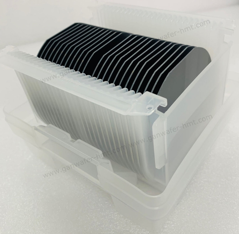
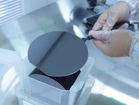
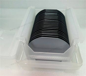
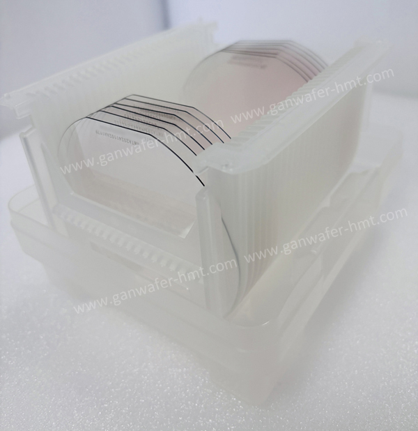
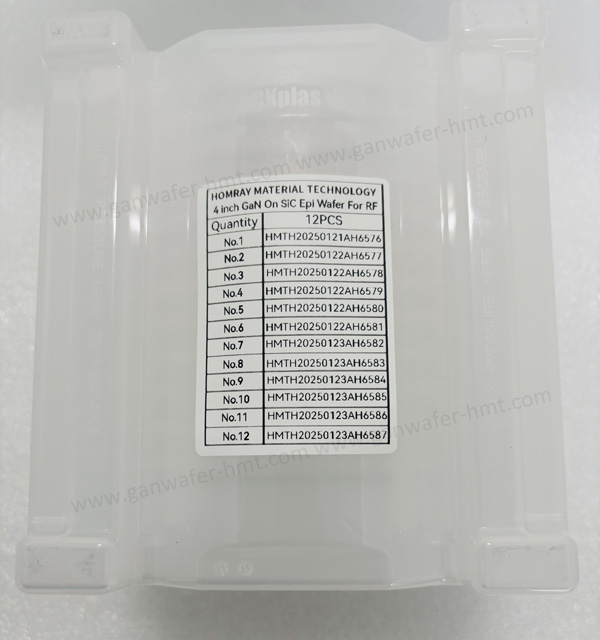
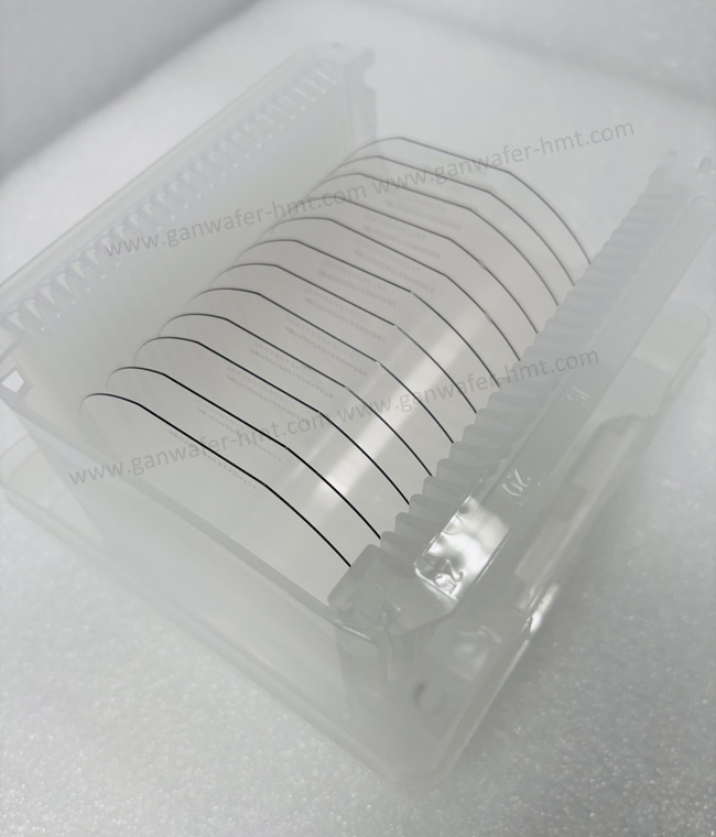
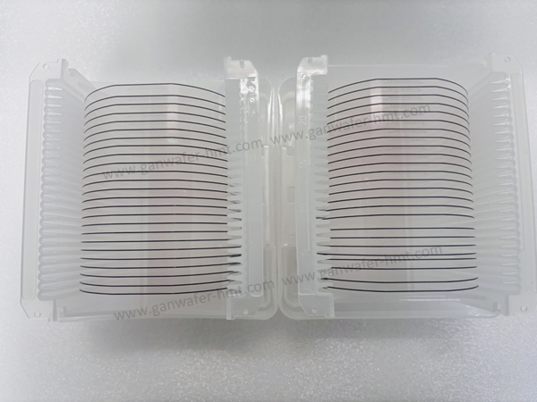
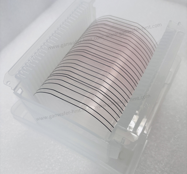
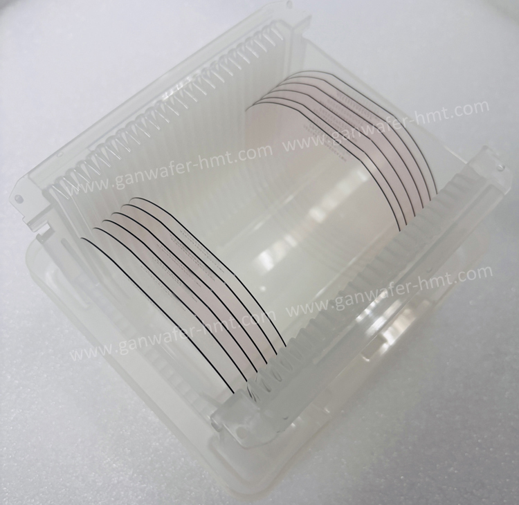
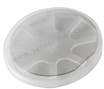
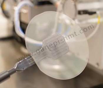
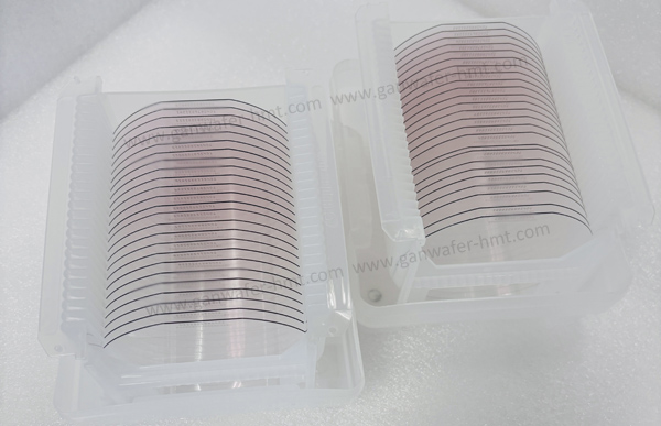
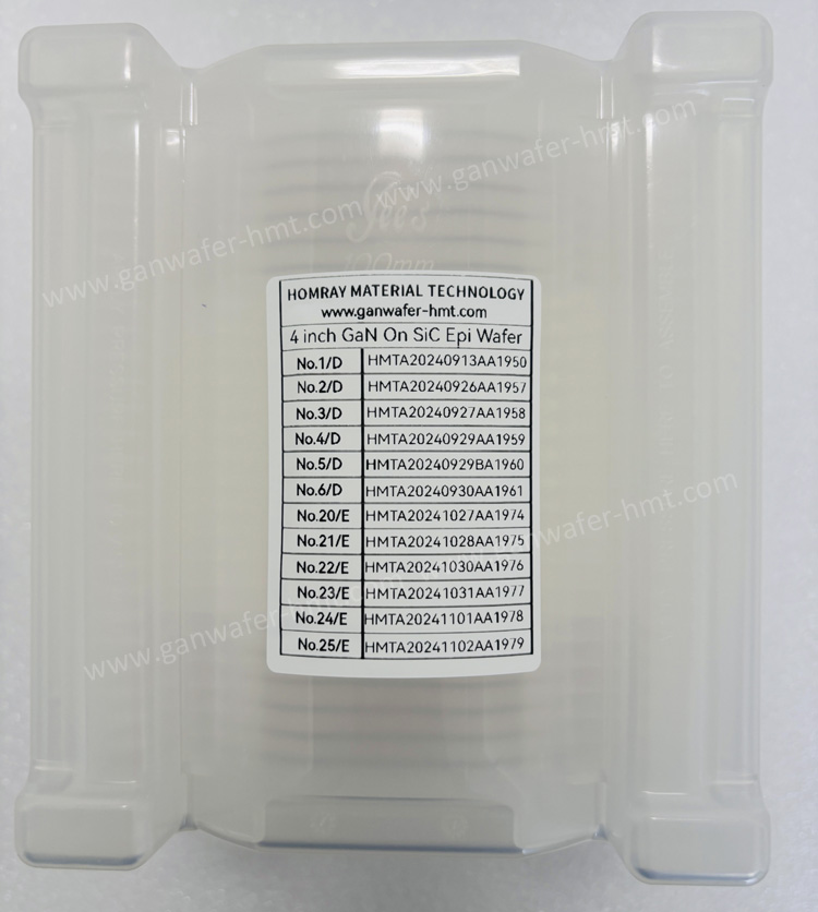
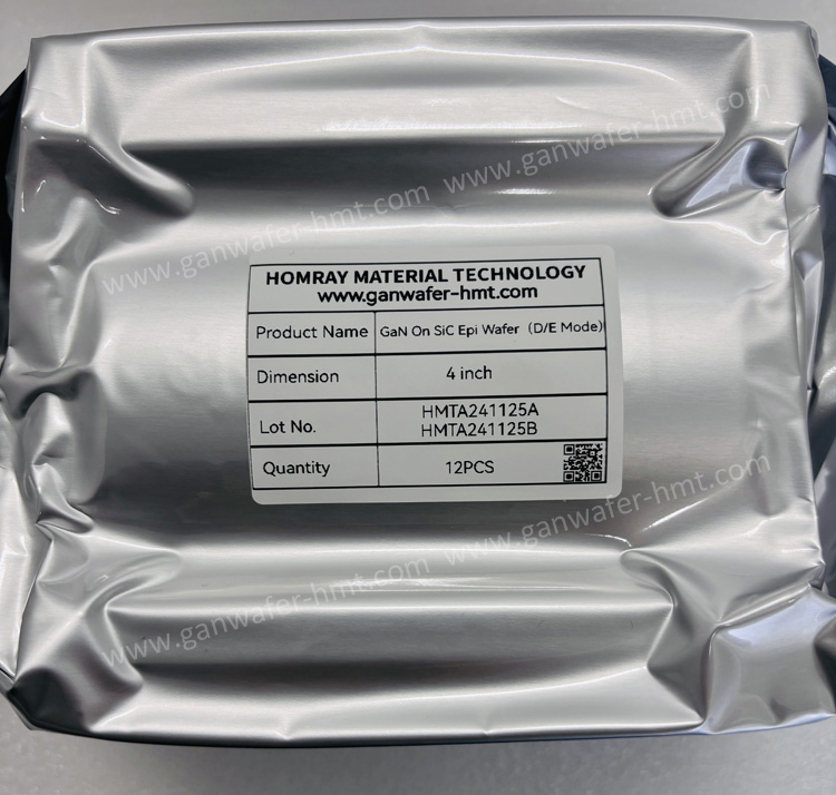
Package Picture of GaN on Si Epi Wafer
Related Products

![]() E-mail: kim@homray-material.com;tina@homray-material.com
E-mail: kim@homray-material.com;tina@homray-material.com
HMT Silicon Carbide (SiC) Wafer Website: www.sicwafer-hmt.com