
GaN Cap AlGaN on Si Epi Wafer Supplier
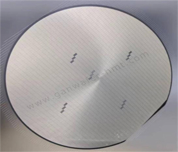
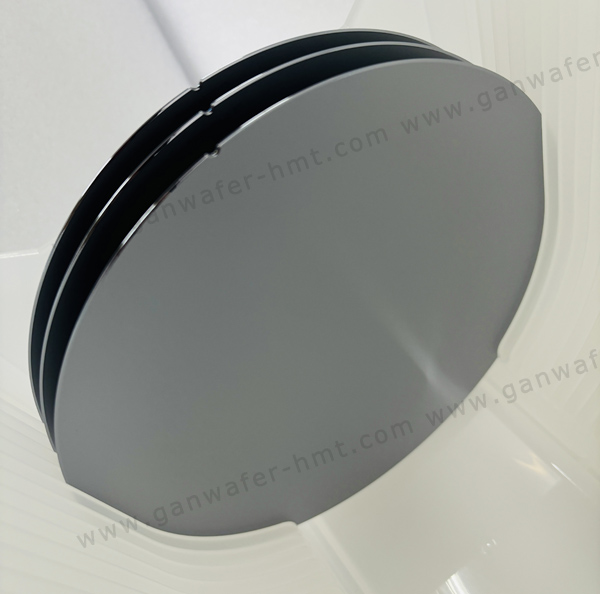
GaN-On-Si Epi Wafer
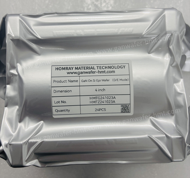
Substrate Size: 4 inch,6 inch,8 inch
Substrate Thickness: 675um,1000um
GaN Cap Thickness: 0-5nm
Product Description
Premium GaN/AlGaN on Si Epi Wafers with SiN or GaN Cap – Customized for Your Needs. As a leading GaN epitaxy wafer supplier in China, we specialize in advanced MOCVD-grown GaN, AlGaN, and SiN cap layers on Silicon substrates, tailored for high-performance RF, power electronics, and optoelectronic applications. With decades of epitaxial growth expertise, we deliver wafers in 4-inch, 6-inch, and 8-inch sizes, combining scalability with precision engineering.
Key Offerings:
-
Structures: D-HEMT, E-HEMT, and custom heterojunction designs with SiN or GaN capping layers.
-
Parameter Flexibility: Adjust layer thickness, doping concentration, and stress profiles to meet specific device requirements.
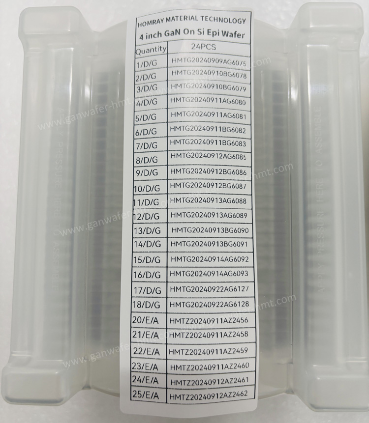
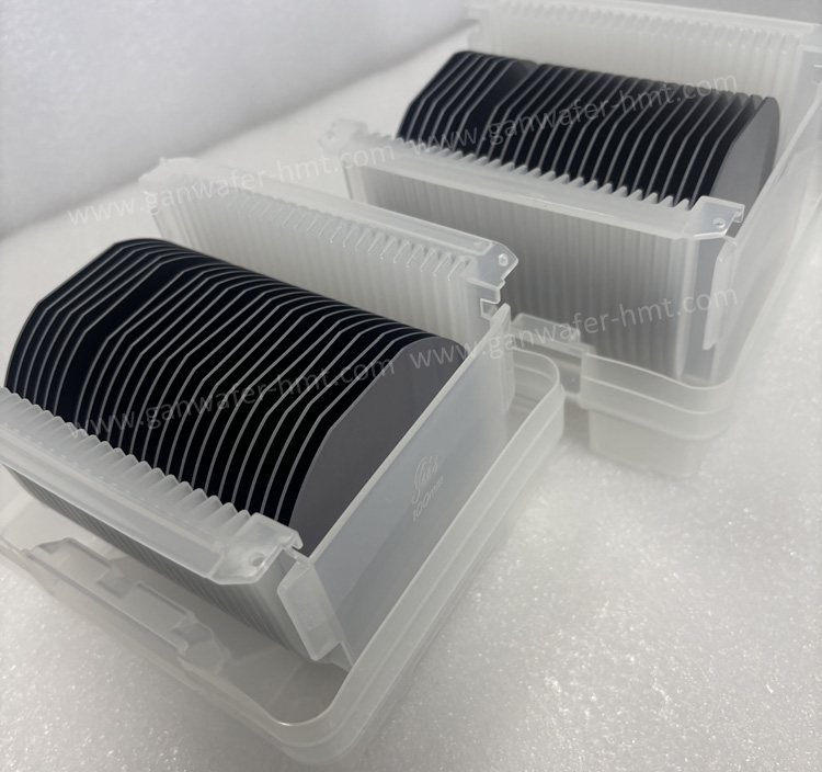
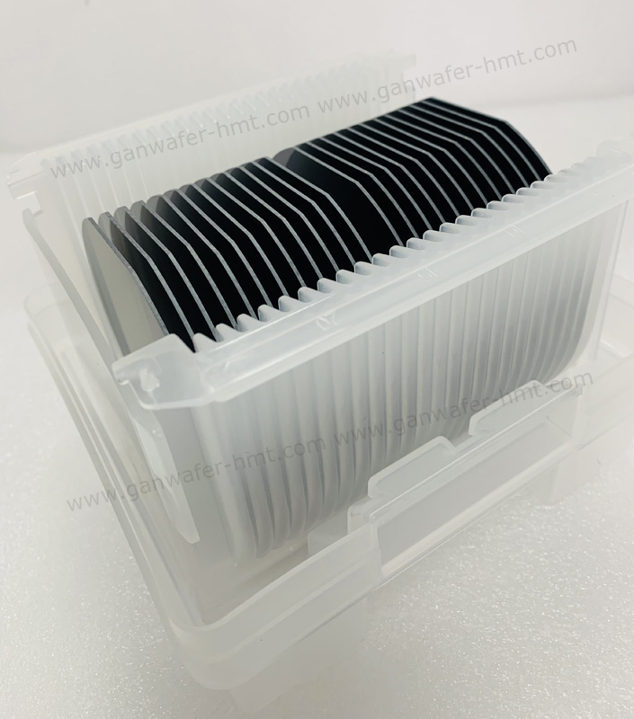
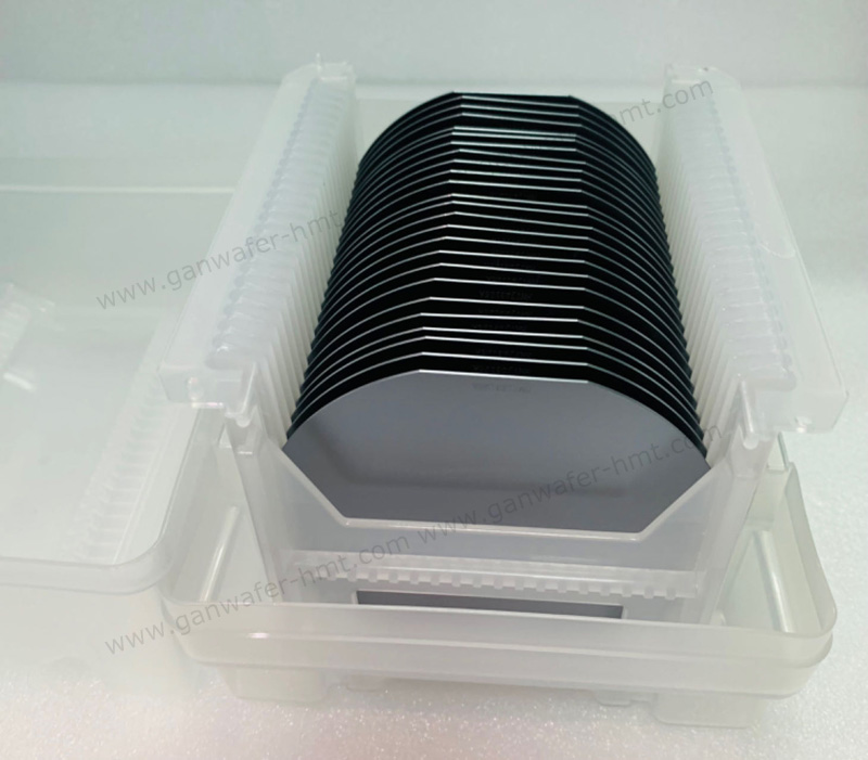
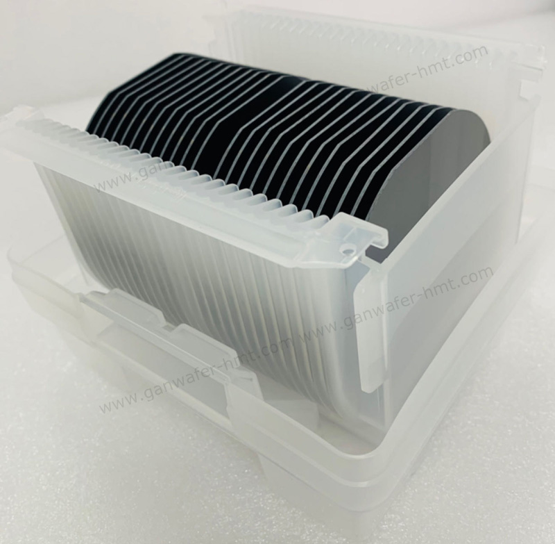
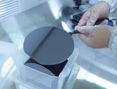
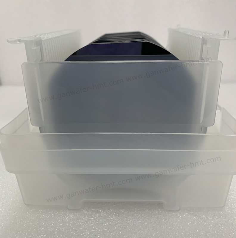
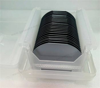
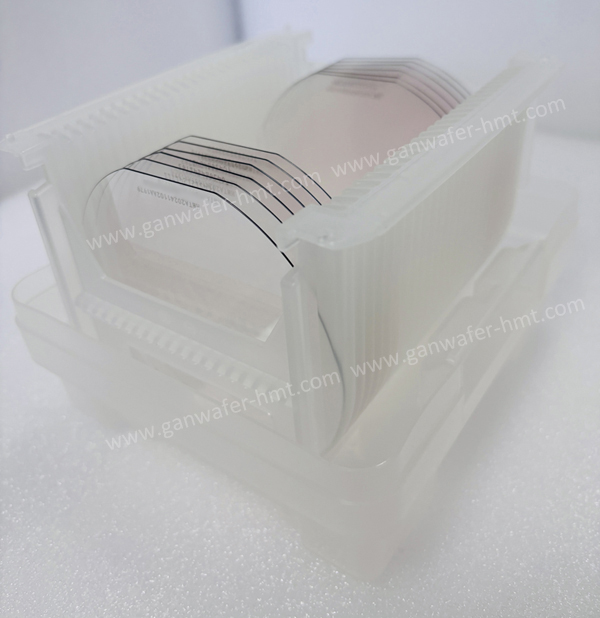
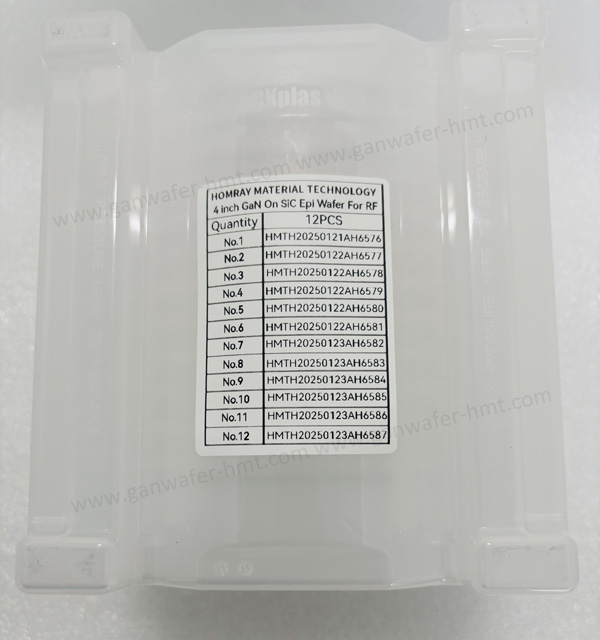
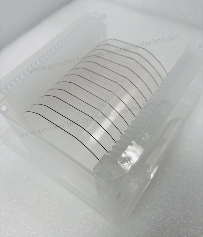
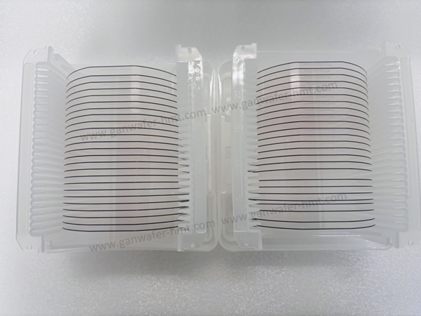
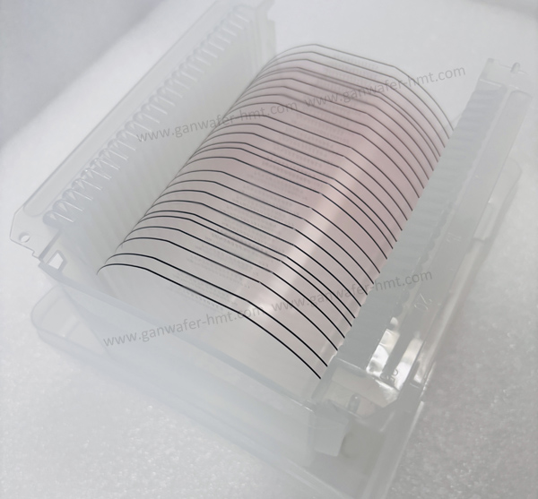
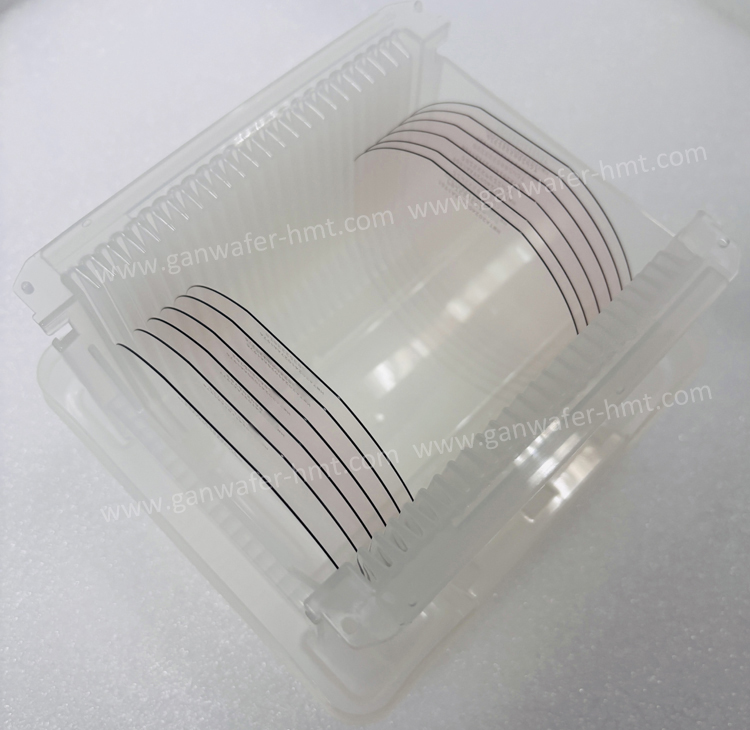
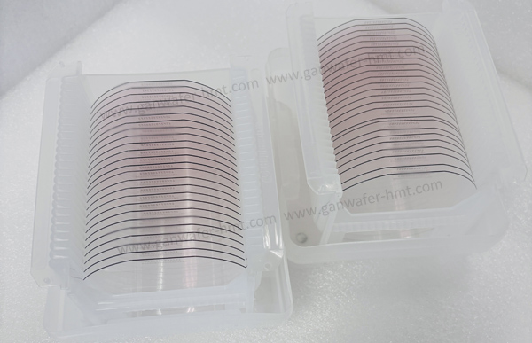
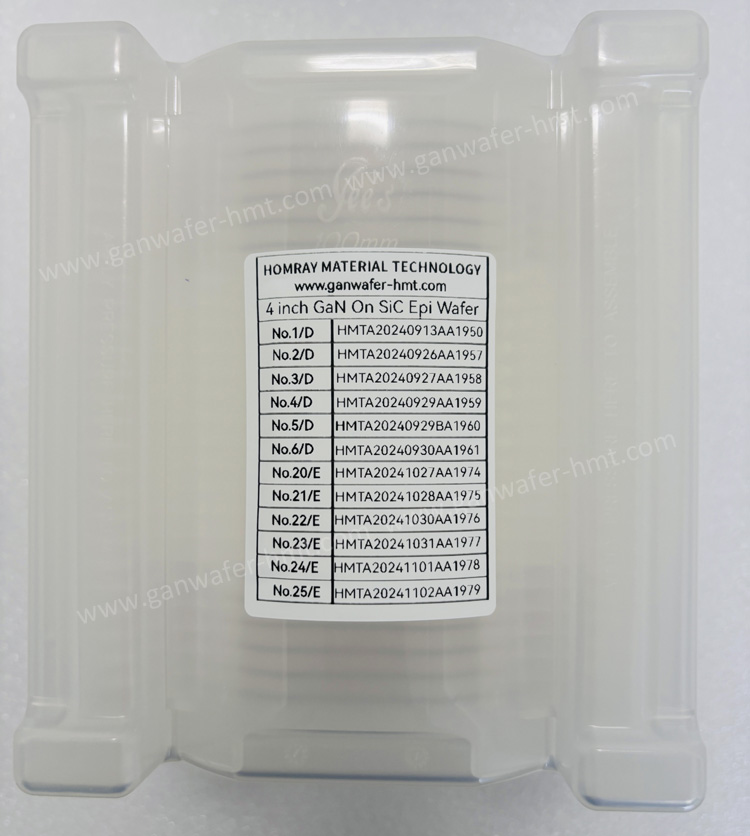
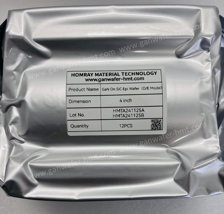
HMT GaN on Si Epi Wafers In Cassette GaN HEMT Chip Class Wafer
-
Why Partner With Us?
✅ End-to-End Support: Our team of PhD-level engineers collaborates with you to optimize epitaxial parameters for peak performance.
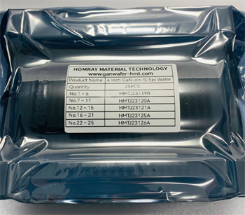
✅ Scalable Production: Seamlessly transition from R&D prototypes to volume orders with batch-to-batch consistency.
✅ Fast Turnaround: Prototype wafers delivered fast, backed by rigorous quality testing.
Request a Quote Today!
Whether you need GaN cap, SiN cap, or AlGaN heterostructures on Si, our solutions bridge innovation and reliability. Contact us to discuss your project’s technical specifications or request sample wafers.
Related Products


![]() M.P: +86-15366208370 ; +86-15366203573
M.P: +86-15366208370 ; +86-15366203573
![]() E-mail: kim@homray-material.com;tina@homray-material.com
E-mail: kim@homray-material.com;tina@homray-material.com
HMT Silicon Carbide (SiC) Wafer Website: www.sicwafer-hmt.com