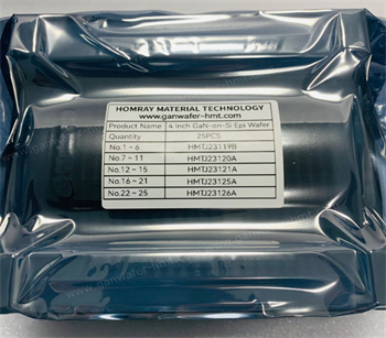
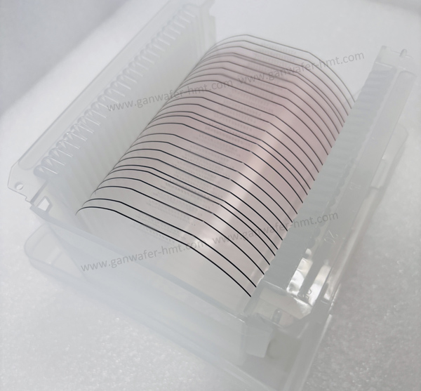
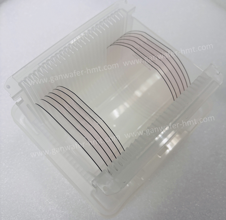
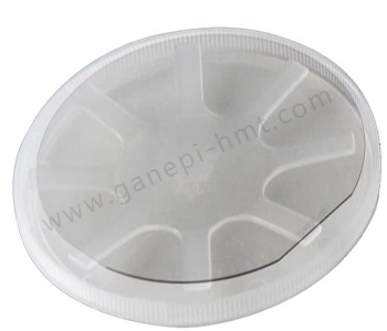
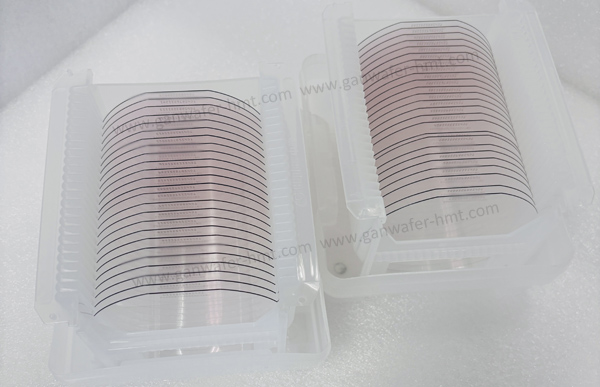
Home | 中文 English
  • Home
  • About Us
  • Products
  • News
  • Success Cases
  • Services
  • Contact Us
  • GaN Substrate Wafer
  • Free-Standing GaN
  • GaN-On-Sapphire Template
  • GaN Epitaxial Wafer
  • GaN HEMT Chip Class Wafer
Home > Products > GaN Epitaxial Wafer > 4/6/8 inch GaN on Si Epi Wafer Manufacturer

4/6/8 inch GaN on Si Epi Wafer Manufacturer

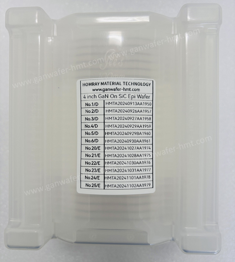
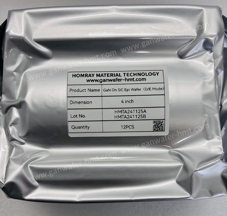
Type: D-Mode/E-Mode/RF
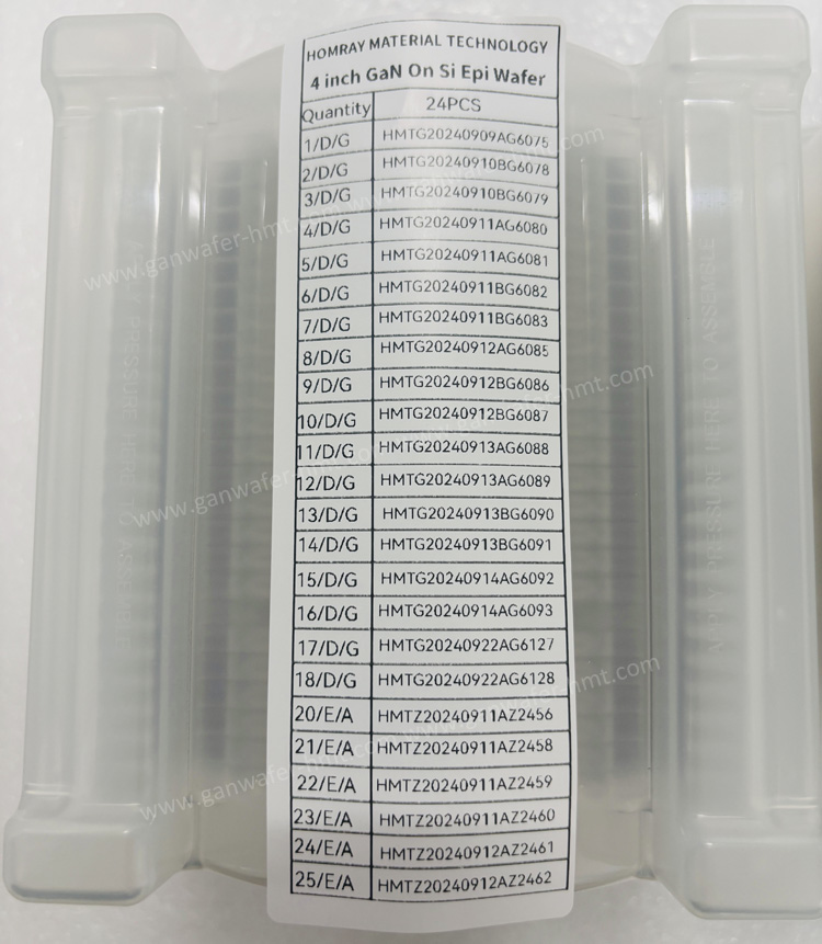
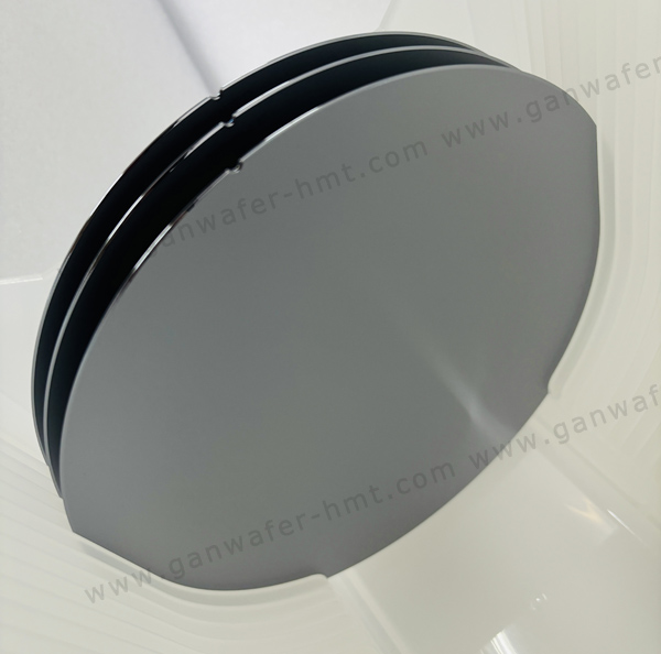
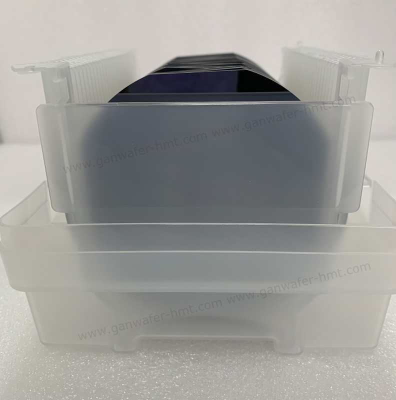
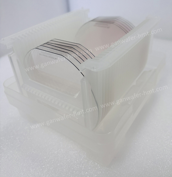
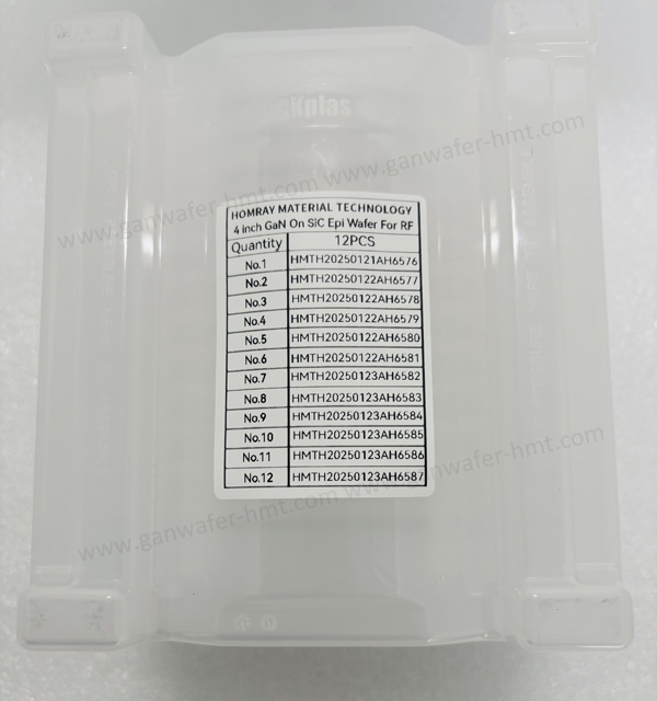
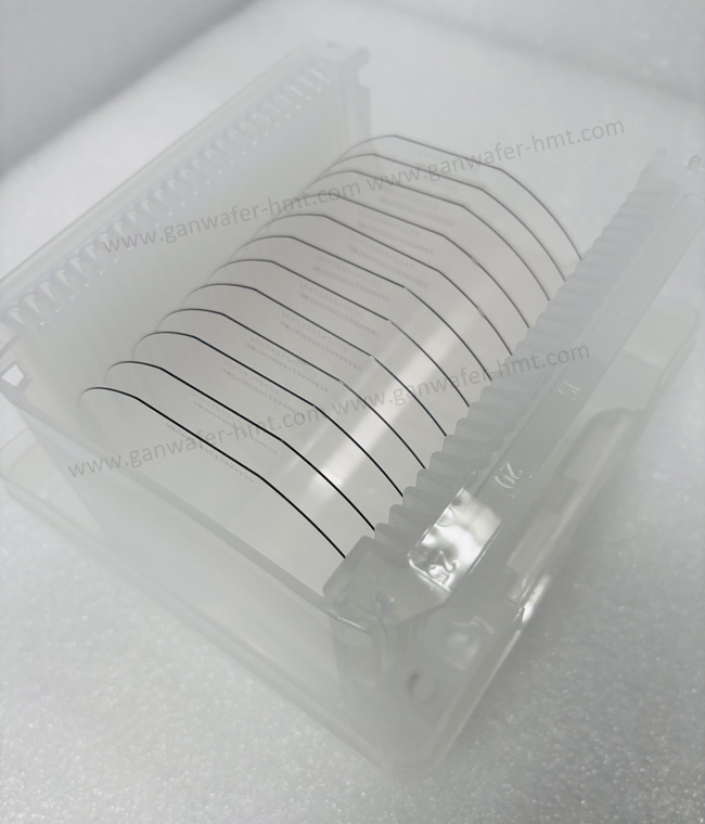
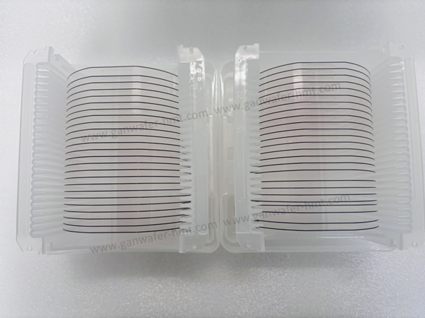
Substrate Diameter: 4-8 inch(111)
Substrate Thickness: 675,1000um
Cap Layer: SiN or GaN Cap

Product Description

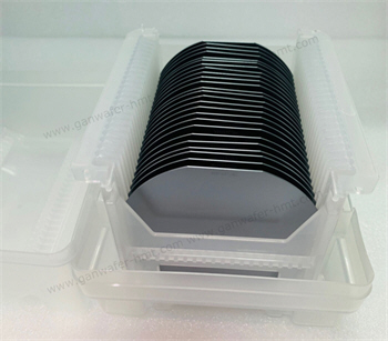
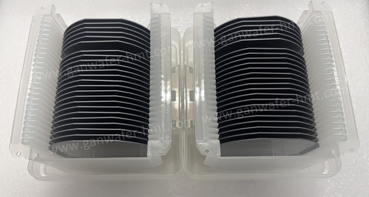
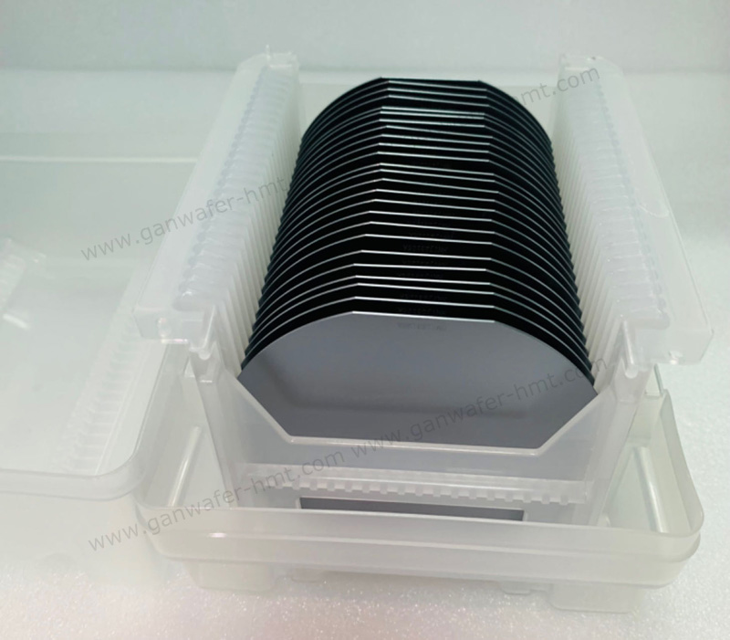
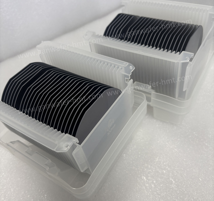
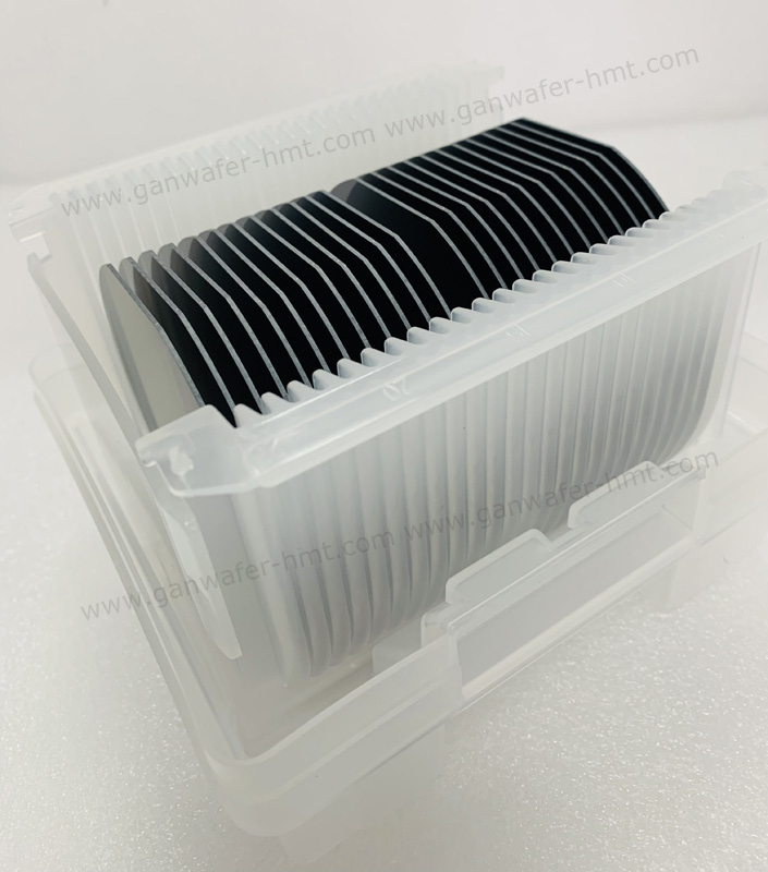
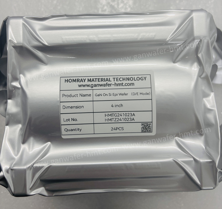
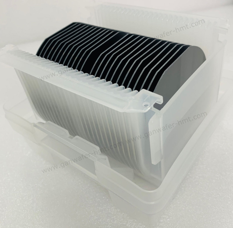
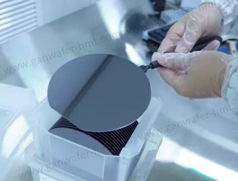
As a premier GaN Epi Wafer Manufacturer, we deliver advanced 4-inch, 6-inch, and 8-inch GaN-on-Si Epi Wafers include D-Mode/E-Mode and RF structure tailored for high-frequency, high-power applications. Our epitaxial solutions are engineered to meet the demands of next-generation technologies, including 5G infrastructure, electric vehicles, and renewable energy systems.

Key Offerings:

  1. Multi-Size GaN-on-Si Epi Wafers

    • 4-inch: Ideal for R&D and specialized RF applications, offering cost-effective prototyping for emerging technologies.

    • 6-inch: Optimized for mass production of power electronics and RF devices, balancing performance and scalability.

    • 8-inch: Designed for high-volume manufacturing, reducing costs while maintaining superior thermal and electrical properties for automotive and industrial markets.

Optoelectronics  
Representative Applications: LEDs, lasers, photodetectors  
Key Advantages: High luminous efficiency, high brightness, long lifespan  
Implementation Scenarios: Lighting, displays, automotive headlights, communication signal lights, medical devices  
GaN-based LEDs have become the material of choice for high-performance lighting equipment due to their superior performance.  

Radio Frequency (RF) Applications 
Representative Applications: 5G communication base stations, satellite communications, military radar  
Key Advantages: High power density, high frequency, high efficiency  
GaN RF devices are becoming a critical foundation for 5G wireless communication infrastructure and defense systems.  

Power Electronics
Representative Applications: Fast-charging devices, new energy vehicles, photovoltaic inverters, power management systems  
Key Advantages: Low energy consumption, high switching speed, high power density  
For example, in fast-charging technology, GaN power devices significantly improve charging efficiency while reducing heat generation and energy consumption.  

High-Frequency Microwave Devices
Representative Applications: High-power amplifiers, power switches, radar systems  
Key Advantages: High-frequency performance, high voltage resistance, high-temperature tolerance  


Related Products

  • RF GaN on HR Si Epi Wafer Supplier

  • GaN Cap AlGaN on Si Epi Wafer Supplier

  • GaN On Si Epi Wafer Power HEMT Manufacturer

  • 硅基氮化镓外延片-D-Mode耗尽型

  • E-HEMT GaN on Si Epi Wafer Manufacturer

  • 硅基HEMT氮化镓外延片E-Mode增强型

  • p-Cap GaN HEMT On Si Epi Wafer Supplier Mg

  • 8 inch GaN-on-Si Epitaxy Wafer Manufacturer

  • D-HEMT AlGaN/GaN on Si Epi Wafer Supplier

  • 4inch RF GaN Epitaxy on Si Wafer Supplier

  • u-GaN Cap On SiC For Power HEMT Supplier

  • D-Mode/E-Mode GaN on SiC Epi Wafers

  • HEMT GaN On SiC Epi Wafer Manufacturers

  • Power HEMT GaN on SiC Epi Wafer Manufacturer

  • AlGaN/GaN On SiC HEMT Epi Wafer Manufacturer

  • 4英寸碳化硅基氮化镓外延片

  • GaN On SiC Epi Wafer RF HEMT Manufacturer

  • 4 inch RF HEMT GaN-on-SiC Epi Wafer Manufacturer

  • AlGaN/GaN碳化硅基氮化镓外延片

  • GaN On Sapphire Epi Wafer Supplier For HEMT

  • GaN Epitaxial Wafer For LED

  • Home
  • About Us
  • Products
  • News
  • Success Cases
  • Services
  • Contact Us

M.P: +86-15366208370 ; +86-15366203573
E-mail: kim@homray-material.com;tina@homray-material.com
HMT Silicon Carbide (SiC) Wafer Website: www.sicwafer-hmt.com