
GaN On Sapphire Epi Wafer Supplier For HEMT
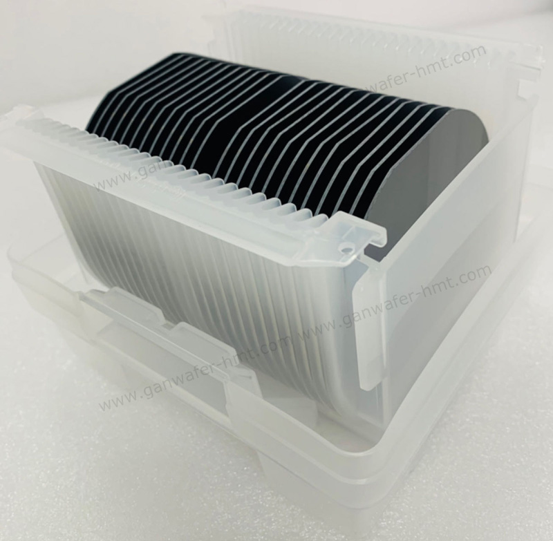
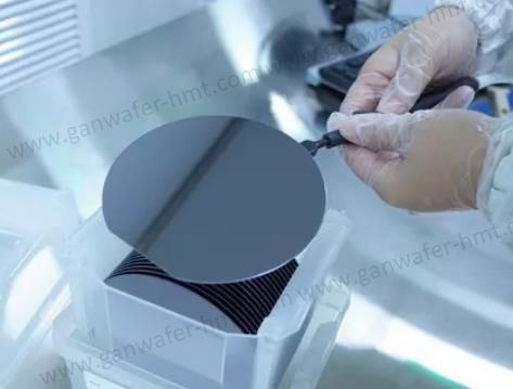
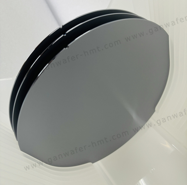
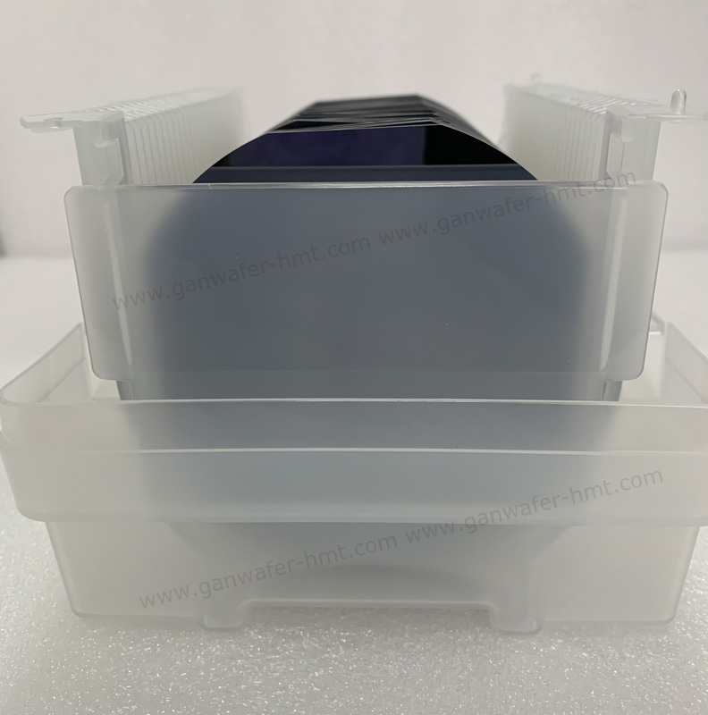
GaN-On-Sapphire Epi Wafer For Power/RF HEMT
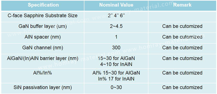
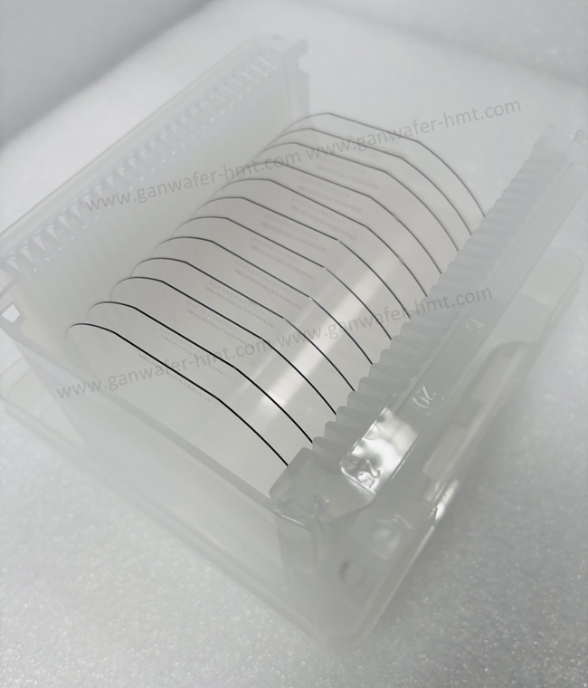
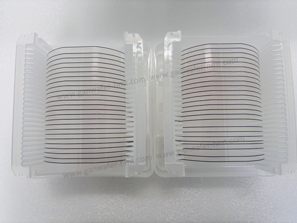
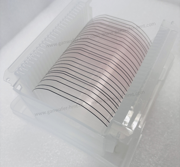
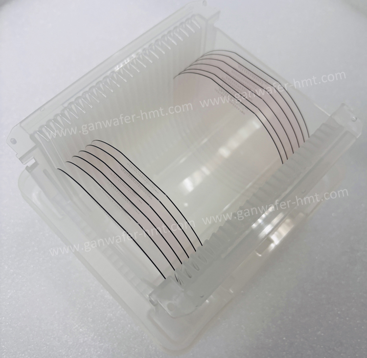
Substrate Size: 2''3''4''6''
Substrate Thickness:430um 520um 650um
GaN Buffer Layer:2-4um
AIN Spacer:1nm
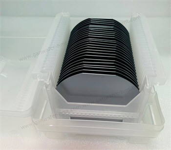
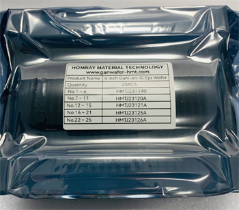
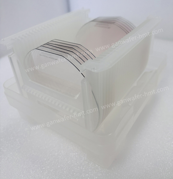
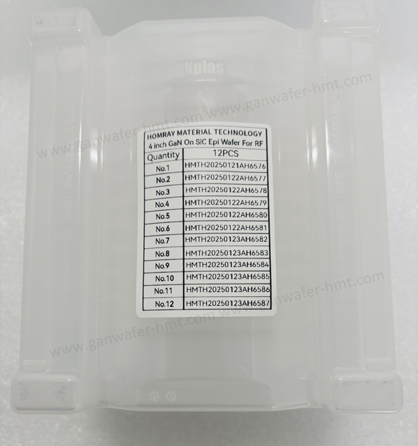
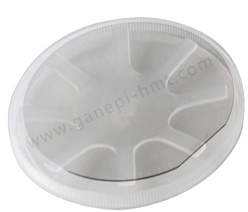
Product Description
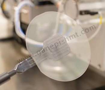
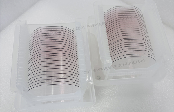
As the leading manufacturer and supplier of GaN (Gallium Nitride) Epi (Epitaxial) wafer and GaN-On-Sapphire Epi Wafer For HEMT/RF HEMT application. Homray Material Technology offers 2inch~6inch GaN (Gallium Nitride) on Sapphire Epi (Epitaxial) wafer for microwave electronic applications. C-face Sapphire substrate thickess is 430um,520um,650um,or 1000~1300um. GaN (Gallium Nitride) buffer layer normal is 2~4um. Homray Material Technology can customized structure and parameters accroding to customers requirement.
GaN technology today is important technology player- Gallium Nitride on Silicon Carbide (GaN on SiC), Gallium Nitride on Silicon (GaN on Si) and Gallium Nitride on Sapphire (GaN on Sapphire). They are used in LED, RF and microwave devices. We can see a dilemma in the GaN supply chain compared with GaAs and its life cycle. Cost-sensitive applications will still go the path of GaAs technology. At the same time, foundries and researchers will service diverse, low-volume applications with specialty GaN processes.
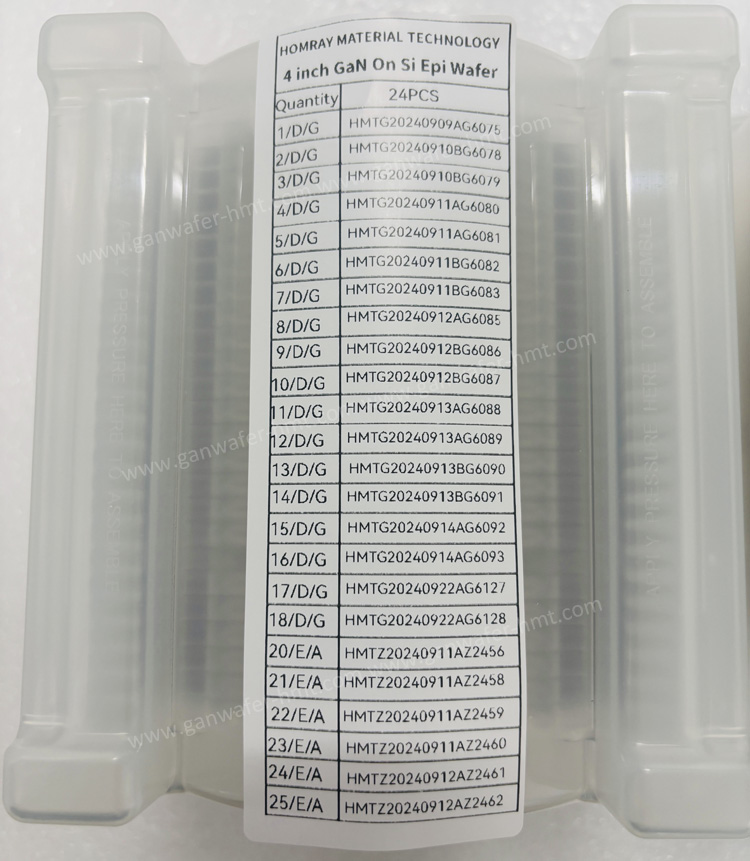
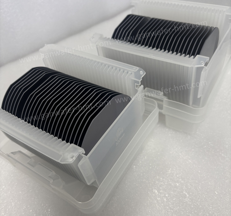
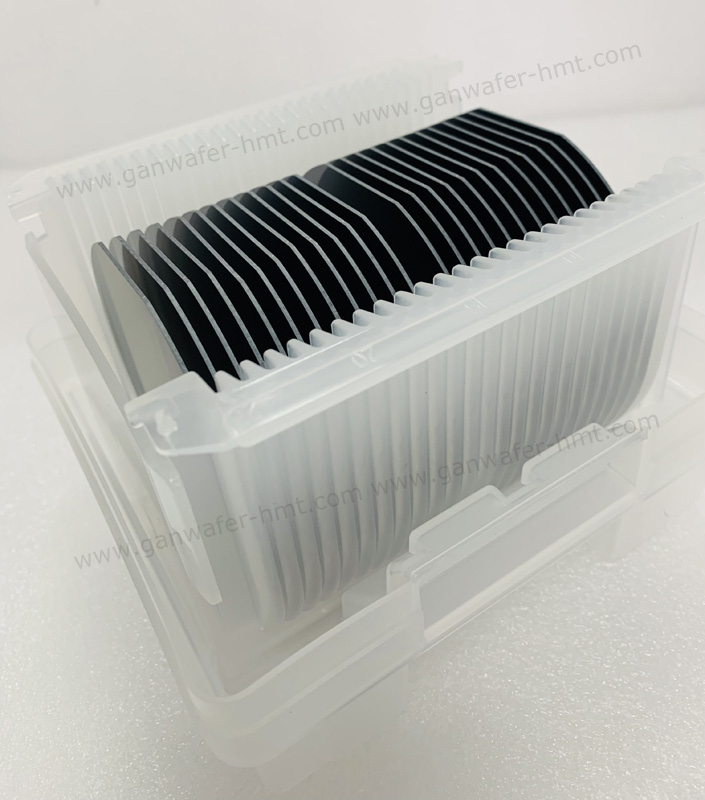
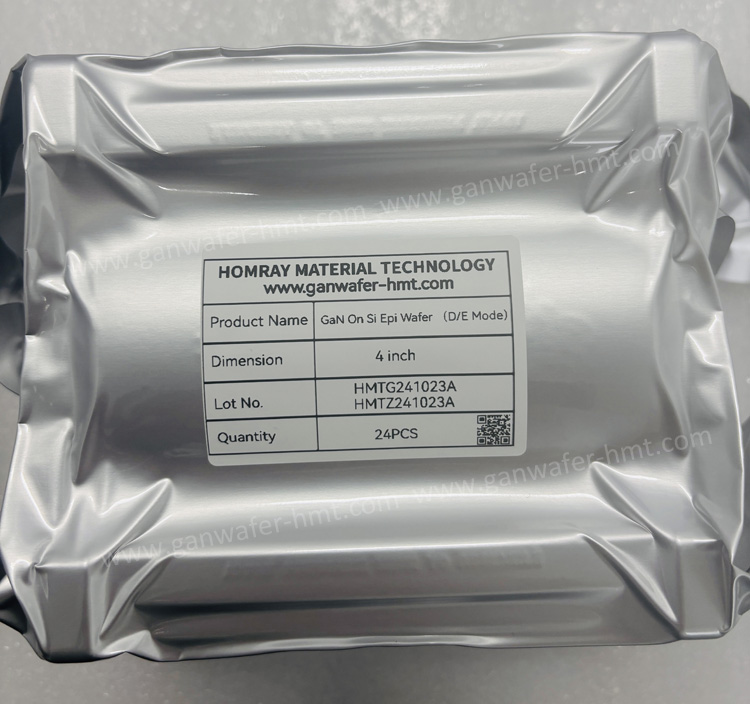
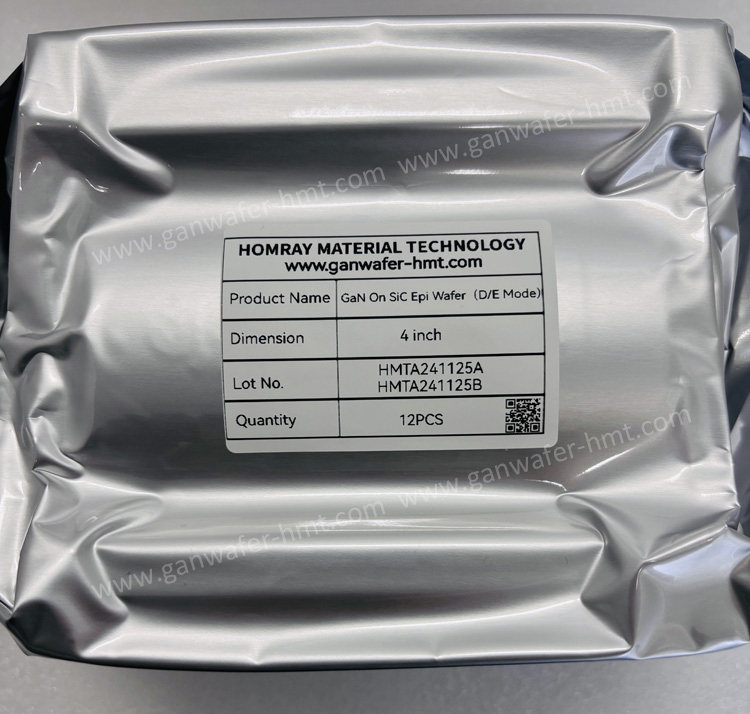
Standard Specification For Power HEMT-D MODE
Please contact us for E MODE and RF HEMT detailed structure.
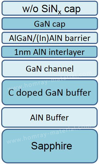
Standard Layer Structure For D mode Applications

Related Products
![]() M.P: +86-15366208370 ; +86-15366203573
M.P: +86-15366208370 ; +86-15366203573
![]() E-mail: kim@homray-material.com;tina@homray-material.com
E-mail: kim@homray-material.com;tina@homray-material.com
HMT Silicon Carbide (SiC) Wafer Website: www.sicwafer-hmt.com