
GaN On SiC Epi Wafer RF HEMT Manufacturer
GaN-On-SiC Epi Wafer For RF HEMT
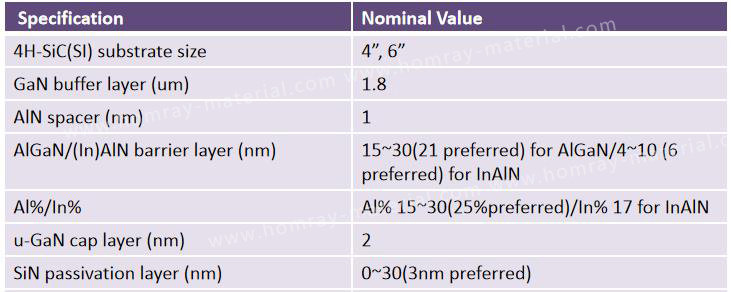
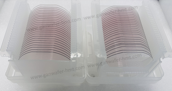
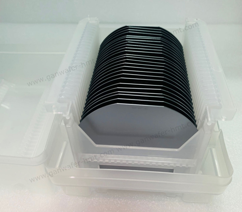
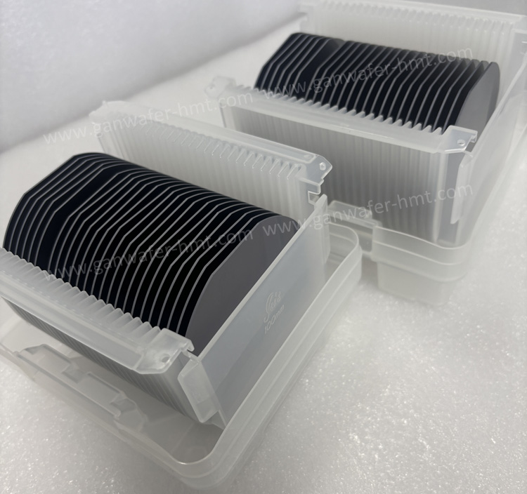
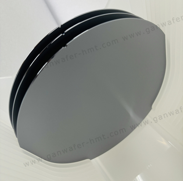
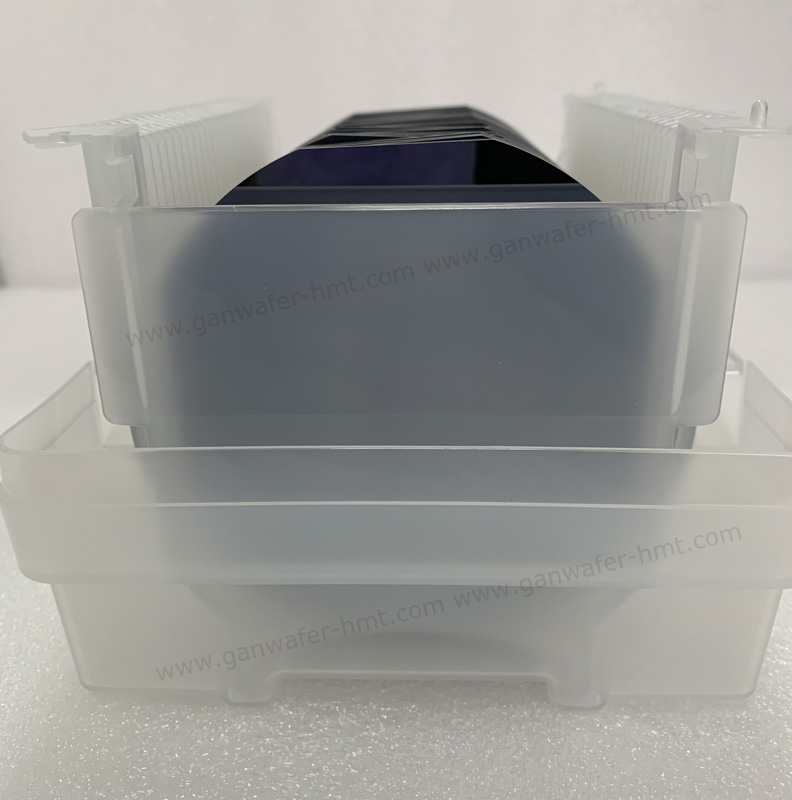
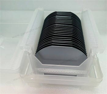
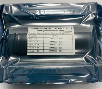
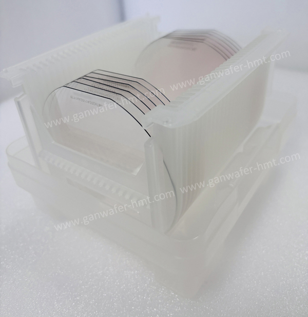
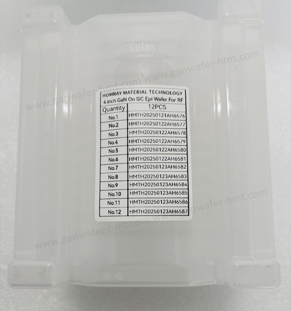
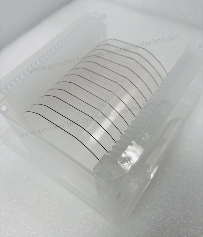
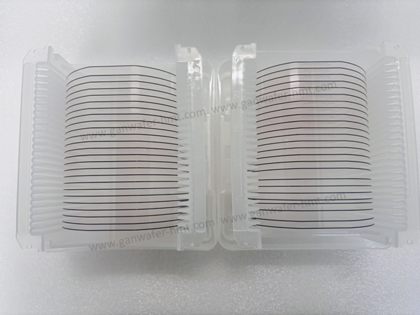
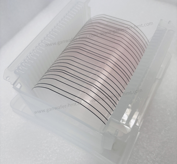
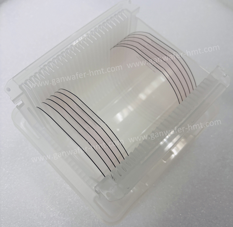
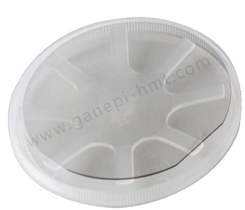
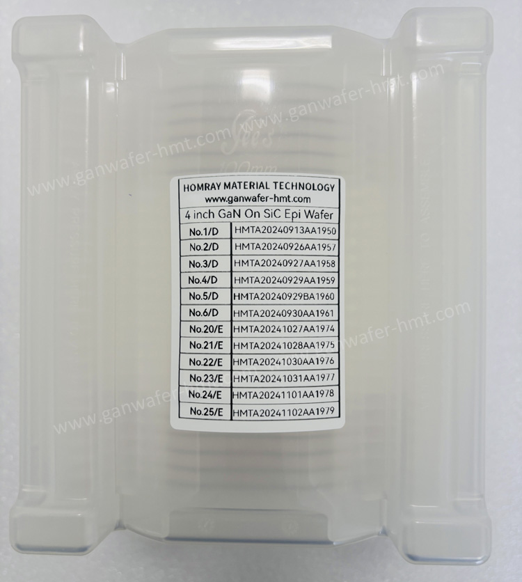
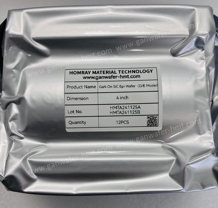
Substrate Size: 4 inch,6 inch
Substrate Thickness: 500um
GaN Buffer Layer: 1.8um
AIN Spacer: 1nm
Product Description
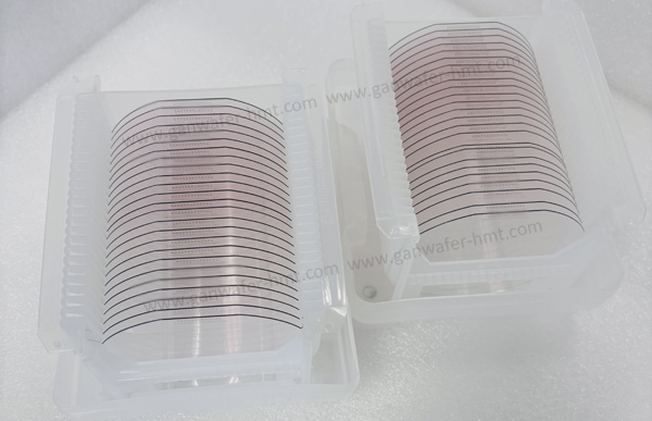
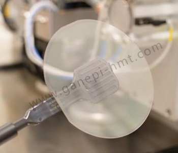
As the leading manufacturer and supplier of GaN (Gallium Nitride) Epi (Epitaxial) wafer and GaN-On-SiC Epi Wafer For RF HEMT application. Homray Material Technology offers 4inch~8inch GaN (Gallium Nitride) on SiC (Silicon Carbide) Epi (Epitaxial) wafer for microwave electronic applications. SiC (Silicon Carbide) substrate thickness is 500um. Gallium Nitride (GaN) HEMTs (High Electron Mobility Transistors) are the next generation of RF power transistor technology.
Gallium Nitride HEMTs are being intensively developed for high-power electronics in high-frequency amplification and power switching applications. Often high performance in DC operation is lost when the HEMT is switched – for example, the on-current collapses when the gate signal is pulsed. It is thought that such effects are related to charge trapping that masks the effect of the gate on current flow. Field-plates on the source and gate electrodes have been used to manipulate the electric field in the device, mitigating such current-collapse phenomena.
Standard Layer Specification For RF HEMT
Please contact us for GaN-on-SiC Power HEMT detailed structure and parameters.
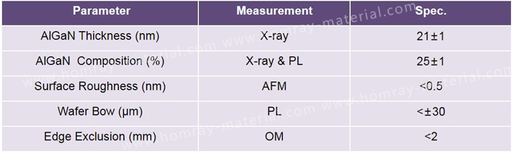
Characterization Specifications
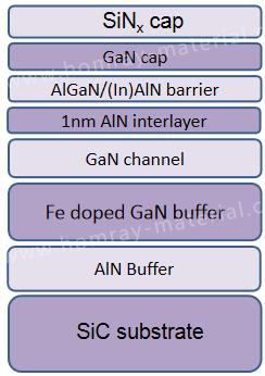
Standard Layer Structure For RF Application

Related Products
![]() E-mail: kim@homray-material.com;tina@homray-material.com
E-mail: kim@homray-material.com;tina@homray-material.com
HMT Silicon Carbide (SiC) Wafer Website: www.sicwafer-hmt.com