
GaN Epi Wafer Manufacturer GaN On SiC/GaN on Si
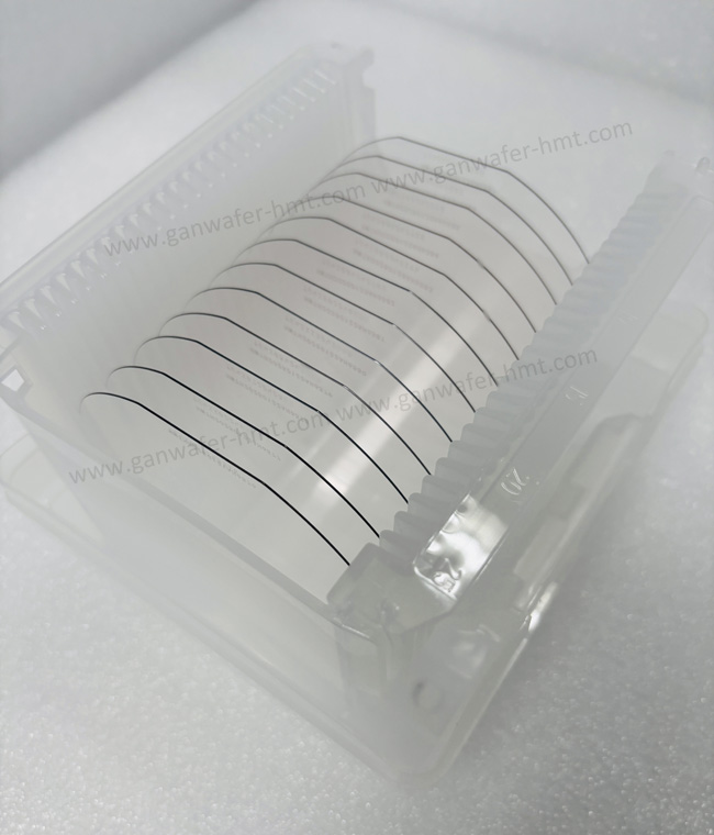
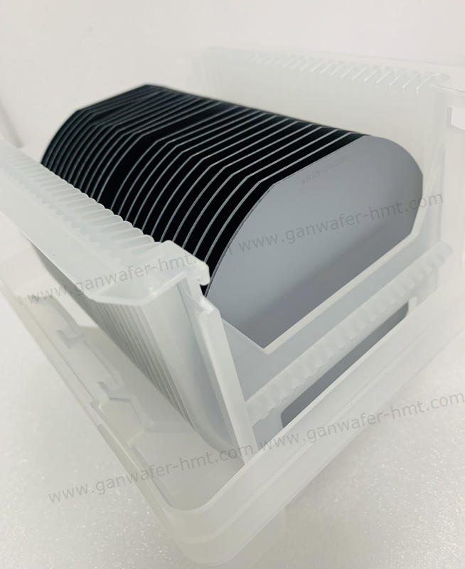
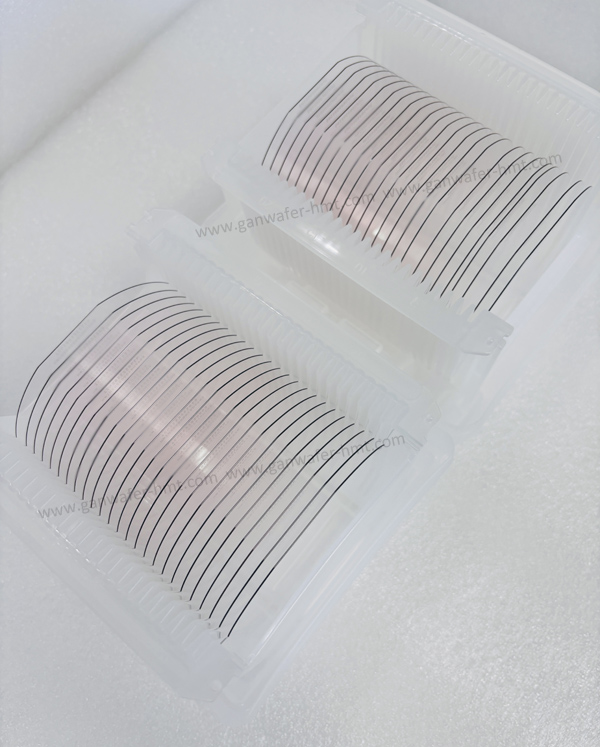
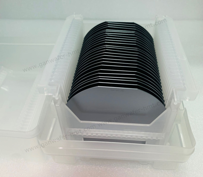
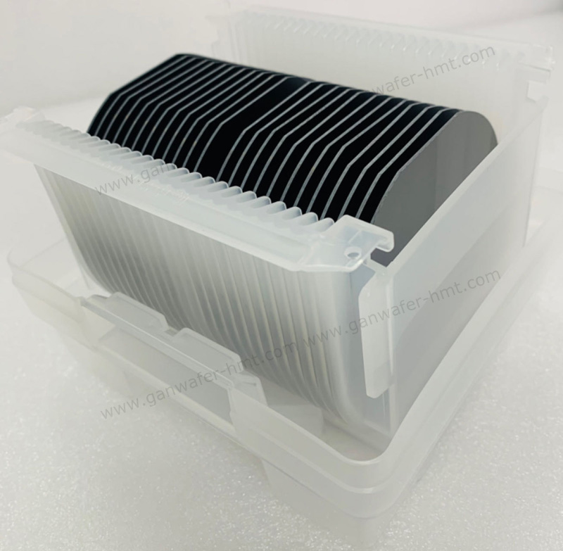
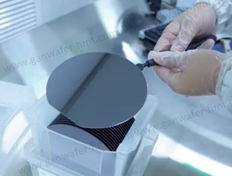
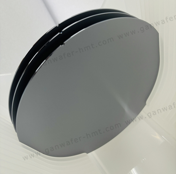
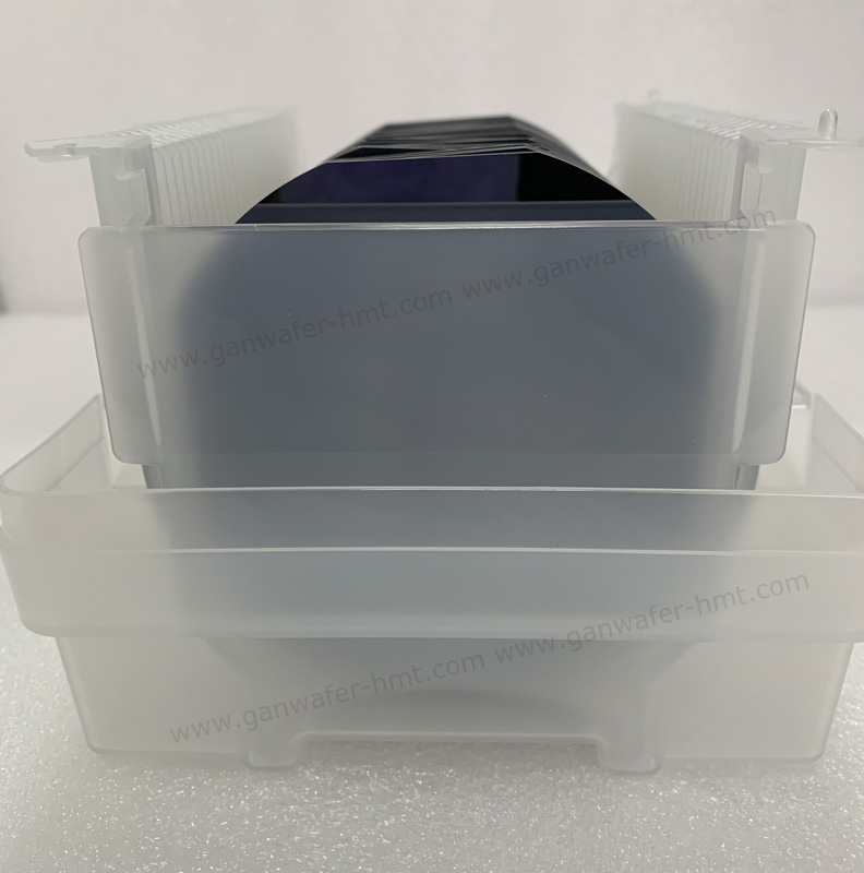
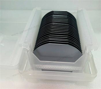
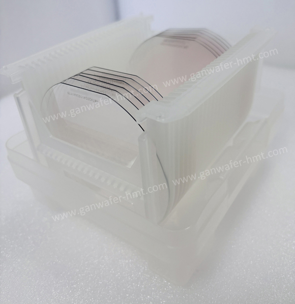
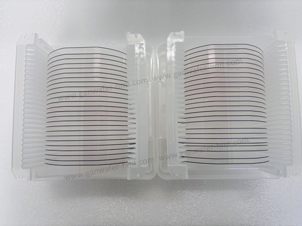
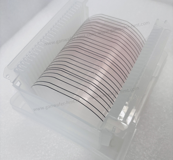
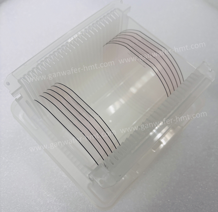
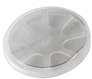
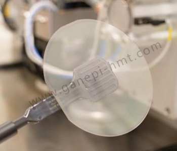
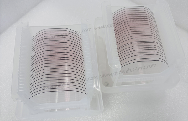
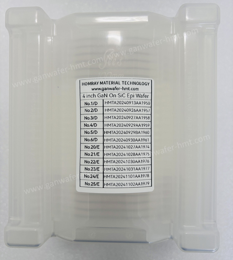
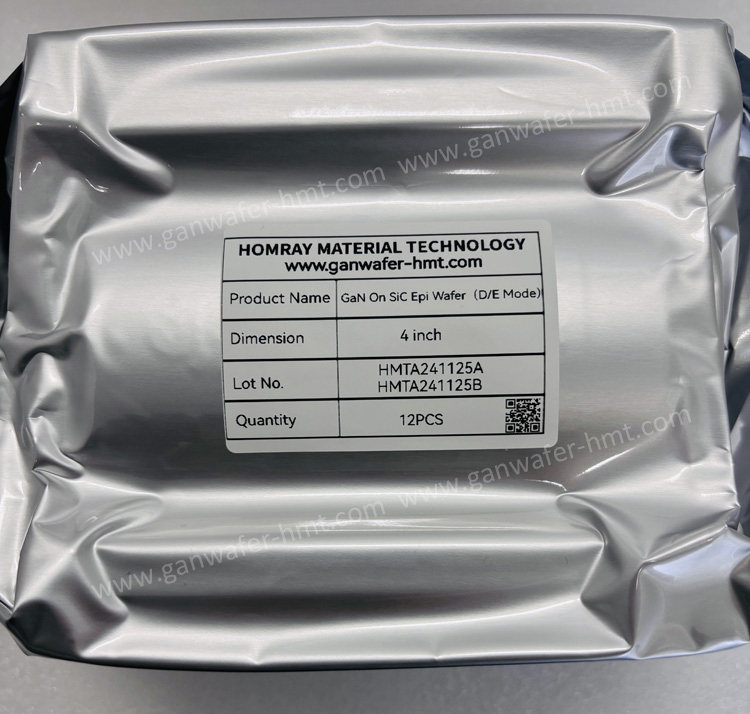
GaN-On-SiC Epi Wafer
Substrate Size: 4 inch,6 inch,8 inch
Substrate Thickness: 500um
Cap Layer: SiN or GaN
Product Description
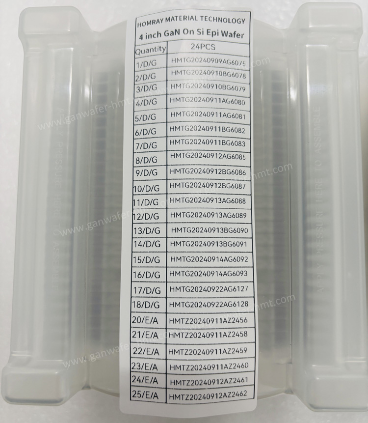
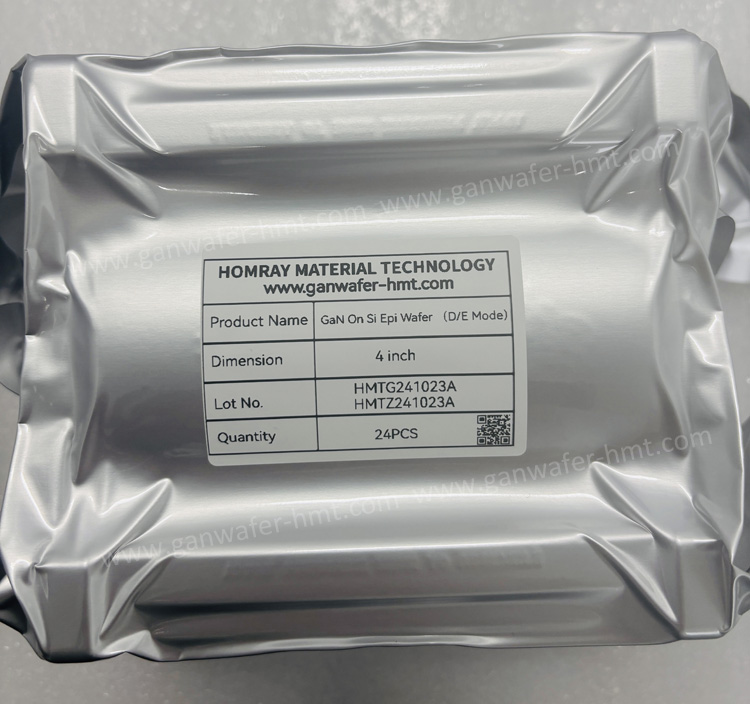
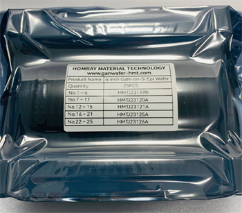
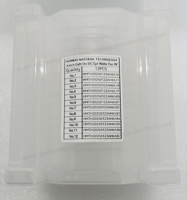
HMT is a leading GaN epi wafer manufacturer supplying high-quality 4'', 6'' and 8'' GaN-on-SiC epitaxial wafers for both RF and Power HEMT applications. Our product line includes GaN HEMT on Si wafers with D-Mode and E-Mode structures. Featuring tunable GaN/SiN cap layers (0-5nm) and precision-doped E-Mode p-GaN (Mg-doped, 90-100nm), HMT delivers advanced solutions for next-generation semiconductor devices.
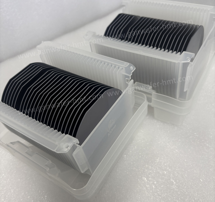
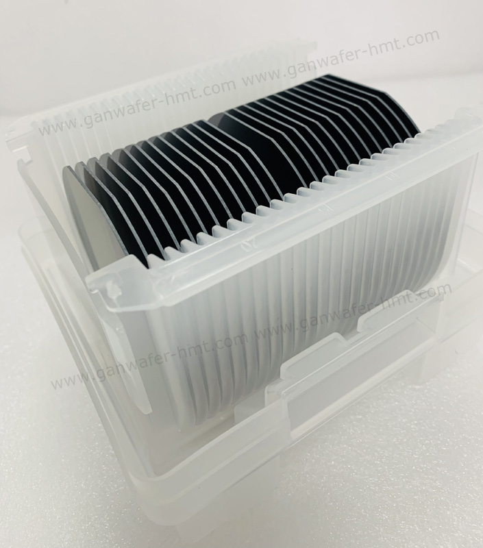
GaN-on-Si Epitaxy Wafer (Silicon Substrate)
Advantages:
Large wafer sizes (mainstream 6-inch and 8-inch), low cost, and mature fabrication process
CMOS compatibility for streamlined integration
Good electrical/thermal conductivity, ideal for cost-effective power integration
GaN-on-SiC Epitaxy Wafer (Silicon Carbide Substrate)
Key Advantages:
-
Low lattice mismatch (~3.5%) and exceptional thermal conductivity (surpassing sapphire/Si), critical for high-power, RF, and high-temperature devices
-
High electrical conductivity enables backside electrodes, optimized for high-frequency/high-voltage applications

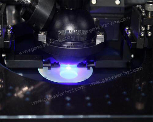
Using Metalorganic Chemical Vapor Deposition (MOCVD) to grow high-quality GaN-based electronic materials on SiC or Si substrates, delivering: -
-
High growth rates with exceptional crystalline quality
-
Superior repeatability and wafer-scale uniformity
Applications & Market Potential
GaN-based microwave power devices and power electronics enable next-generation solutions for:
-
5G/6G mobile communication base stations
-
Advanced RF and energy-efficient power systems
-
Related Products
![]() E-mail: kim@homray-material.com;tina@homray-material.com
E-mail: kim@homray-material.com;tina@homray-material.com
HMT Silicon Carbide (SiC) Wafer Website: www.sicwafer-hmt.com