
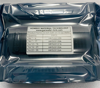
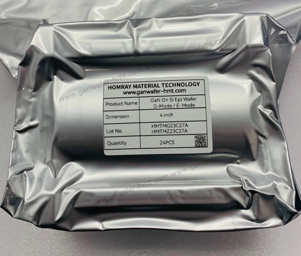
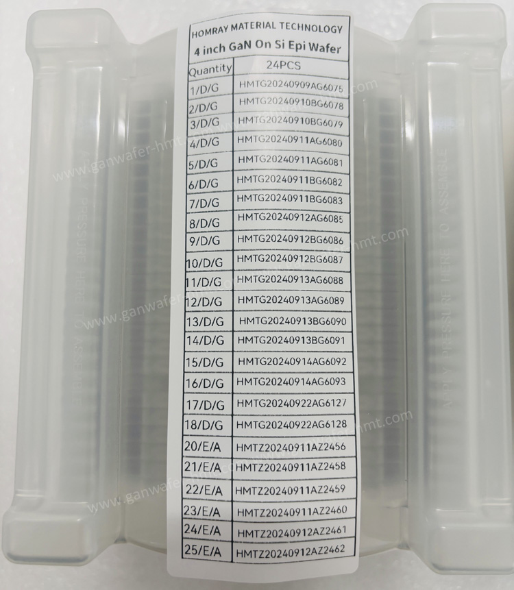
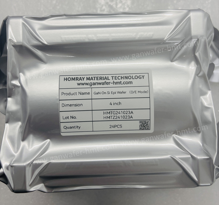
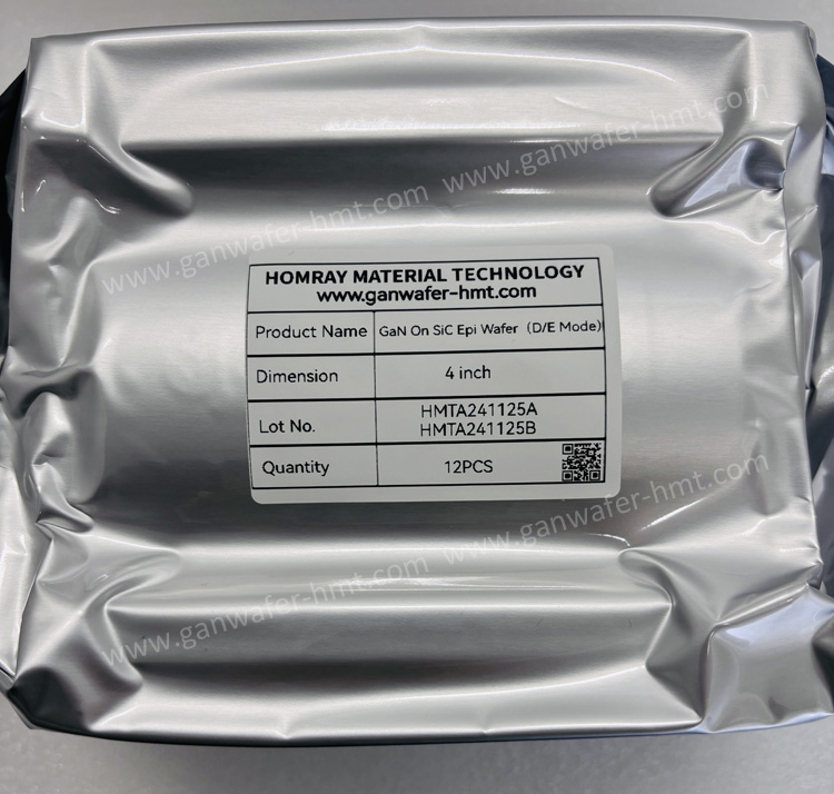
4inch RF GaN Epitaxy On Si Wafer Supplier
Type: D-Mode/E-Mode/RF
Substrate Diameter: 4-8 inch(111)
Substrate Thickness: 675,1000um
Cap Layer: SiN or GaN Cap
Product Description
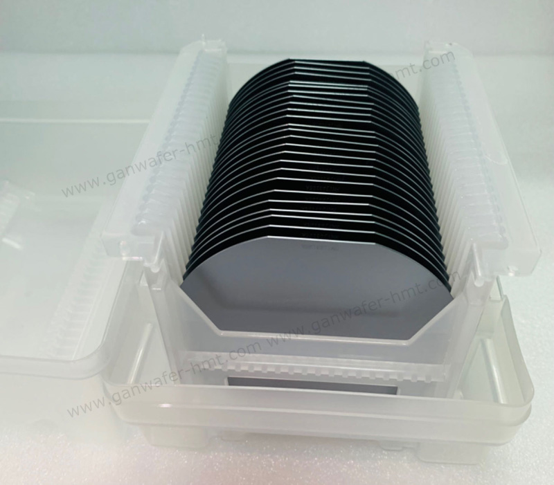
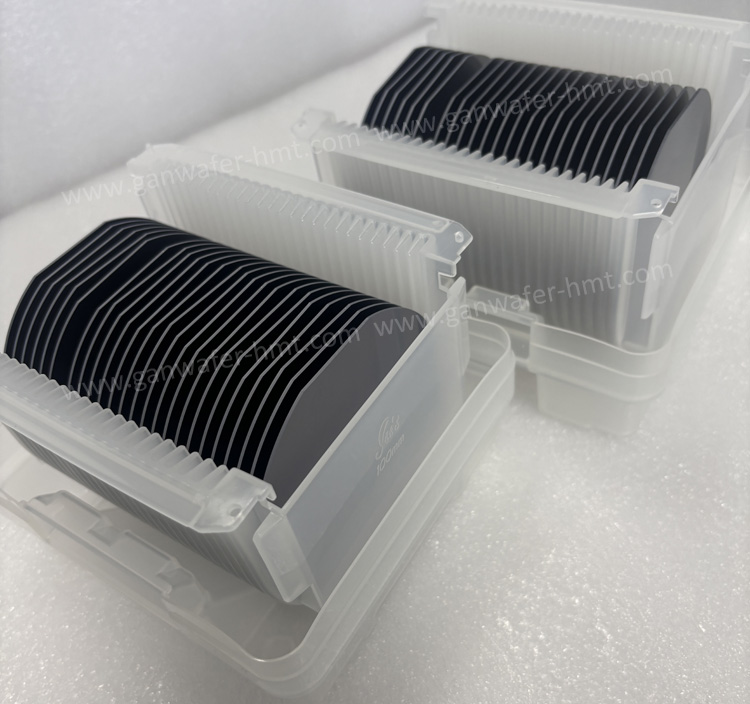
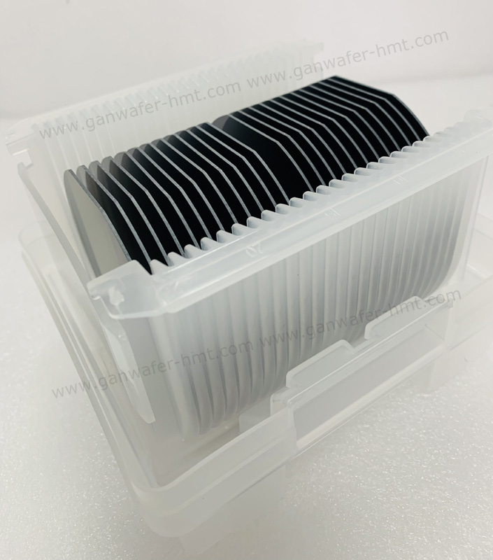
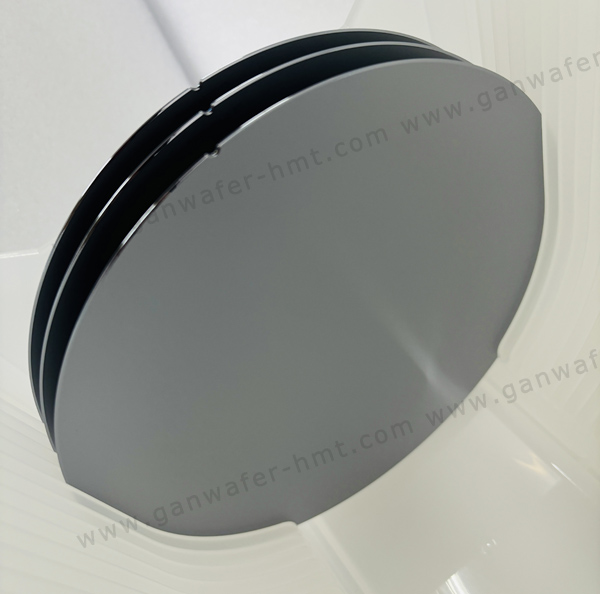
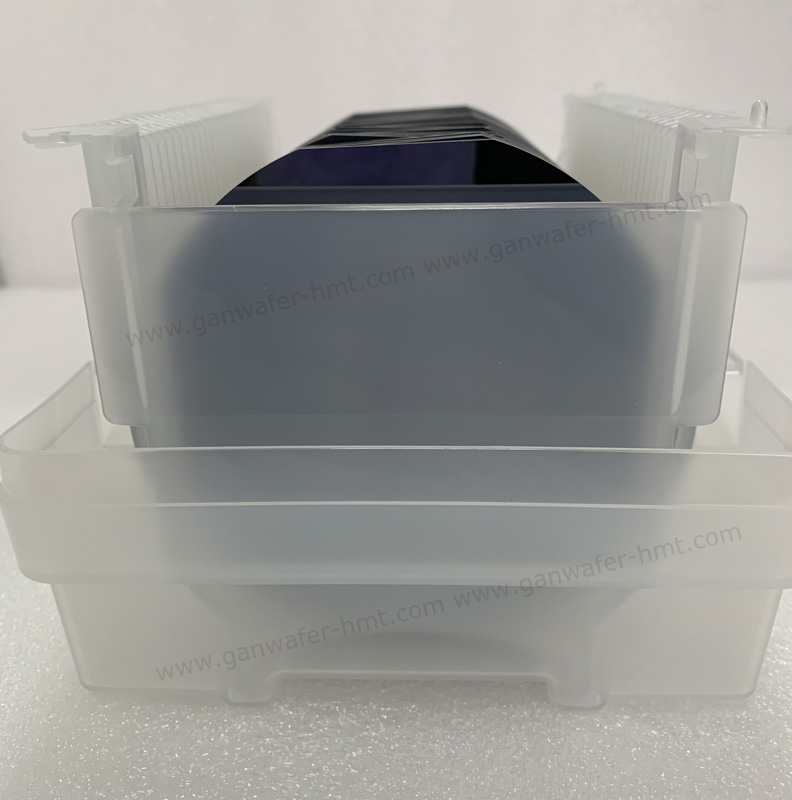
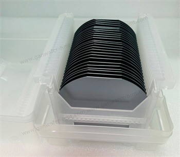
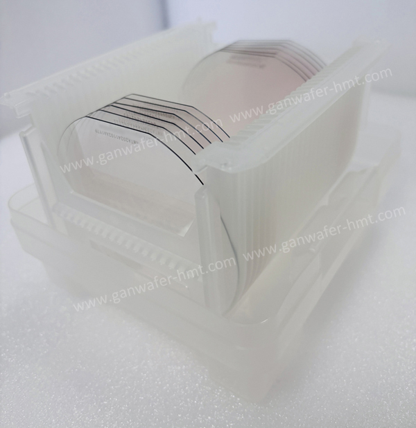
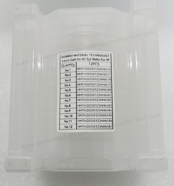
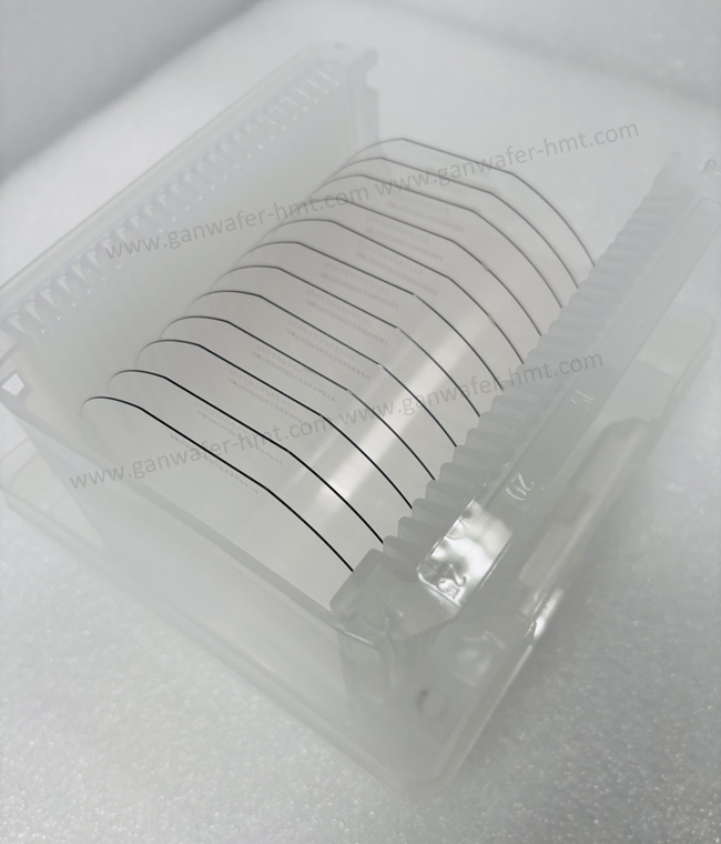
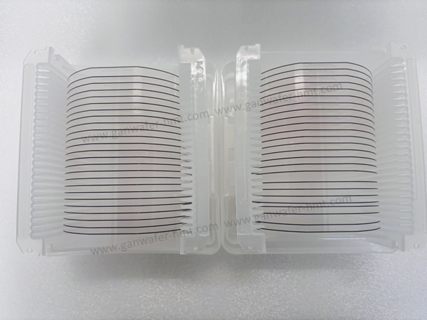
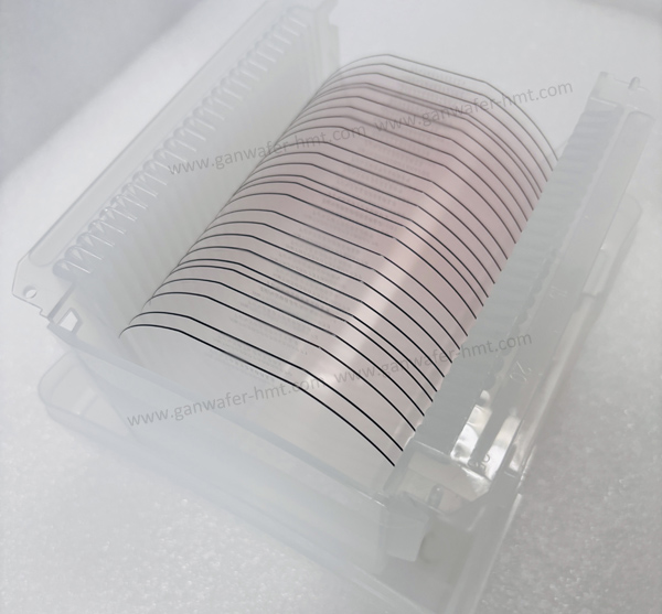
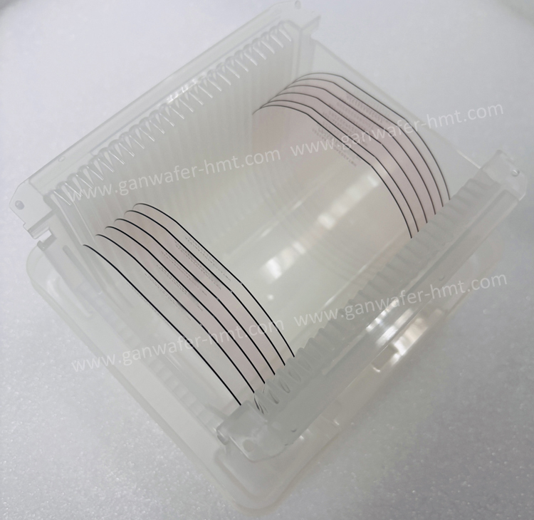
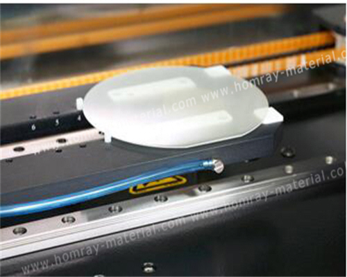
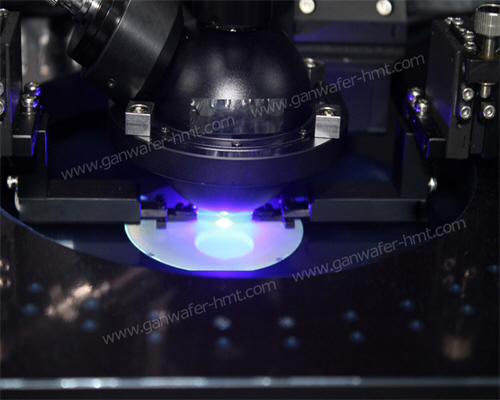
HMT offers high-performance MOCVD-grown GaN on Silicon (GaN-on-Si) epitaxial wafers in 4-inch, 6-inch, and 8-inch configurations, engineered to deliver superior crystal quality, high uniformity, and exceptional reliability at competitive pricing.
Why cooperate with HMT?
-
Rapid wafer customization lead time.
-
Professional engineers optimize customers structural parameters
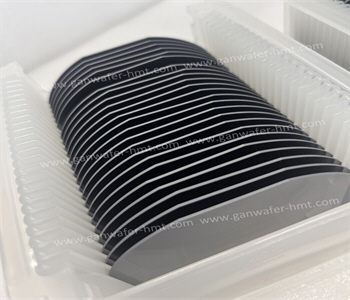
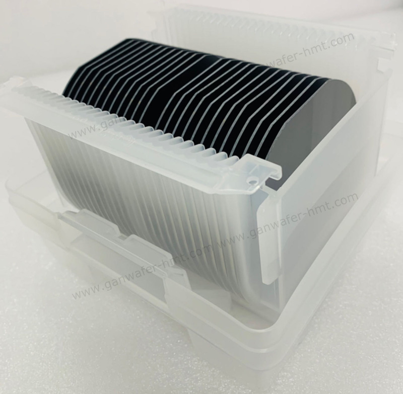
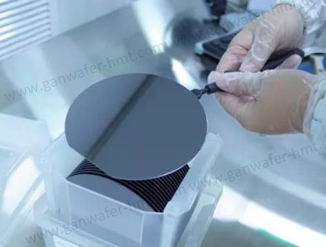
The anti-breakage packaging ensures customers received wafers safe.

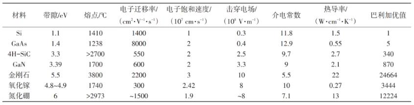
GaN is a third-generation semiconductor material (also known as a wide-bandgap semiconductor material) and holds significant advantages over Si and GaAs in terms of key parameters:
-
The Johnson figure of merit (a comprehensive metric for evaluating semiconductor materials in power and frequency applications) for GaN and GaAs is 27.5 and 2.7, respectively, indicating GaN's clear superiority over GaAs.
-
Compared to GaAs (bandgap: 1.43 eV), GaN has a bandgap of 3.4 eV—approximately 2.4 times wider than that of GaAs.
-
GaN devices exhibit exponentially higher breakdown field strength, enabling operation at higher voltages.
-
GaN materials demonstrate higher carrier drift velocity under high electric fields, allowing for greater operating current. In contrast, while GaAs has high electron mobility at low electric fields and room temperature, its mobility sharply declines and even turns negative under slightly higher electric fields, leading to a drastic drop in carrier drift velocity.
As a material for developing advanced radar systems, jammers, and military electronic components such as T/R modules, gallium nitride (GaN) is now replacing gallium arsenide (GaAs).
For the same volume, GaN offers superior linearity, higher power density (>5 W/mm), better power performance (5–10x improvement), higher supply voltage (~50–70 V), higher saturation current, and broader frequency bandwidth, along with enhanced durability. Additionally, GaN enables stronger radiation power, extends detection range, reduces size and weight, improves mobility and battlefield survivability, shortens maintenance intervals, and enhances radar availability.
Related Products
![]() E-mail: kim@homray-material.com;tina@homray-material.com
E-mail: kim@homray-material.com;tina@homray-material.com
HMT Silicon Carbide (SiC) Wafer Website: www.sicwafer-hmt.com