
HEMT GaN On SiC Epi Wafer Manufacturers
GaN-On-SiC Epi Wafer For Power HEMT
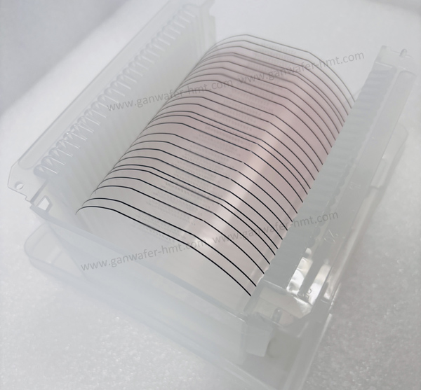
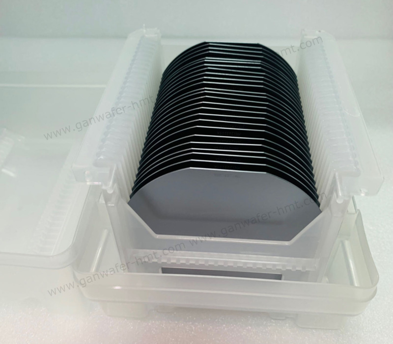
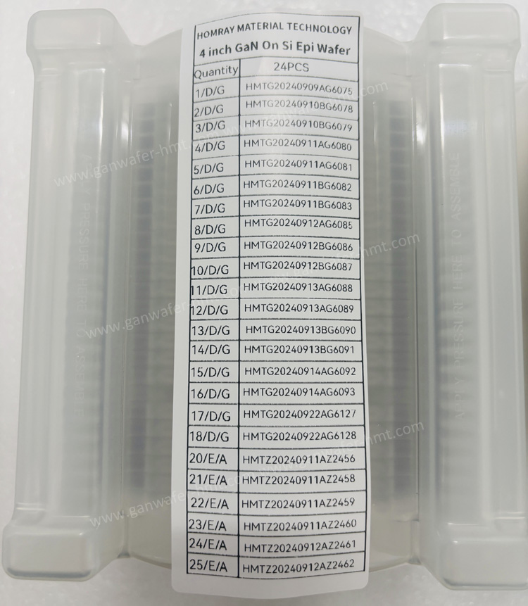
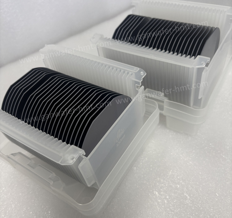
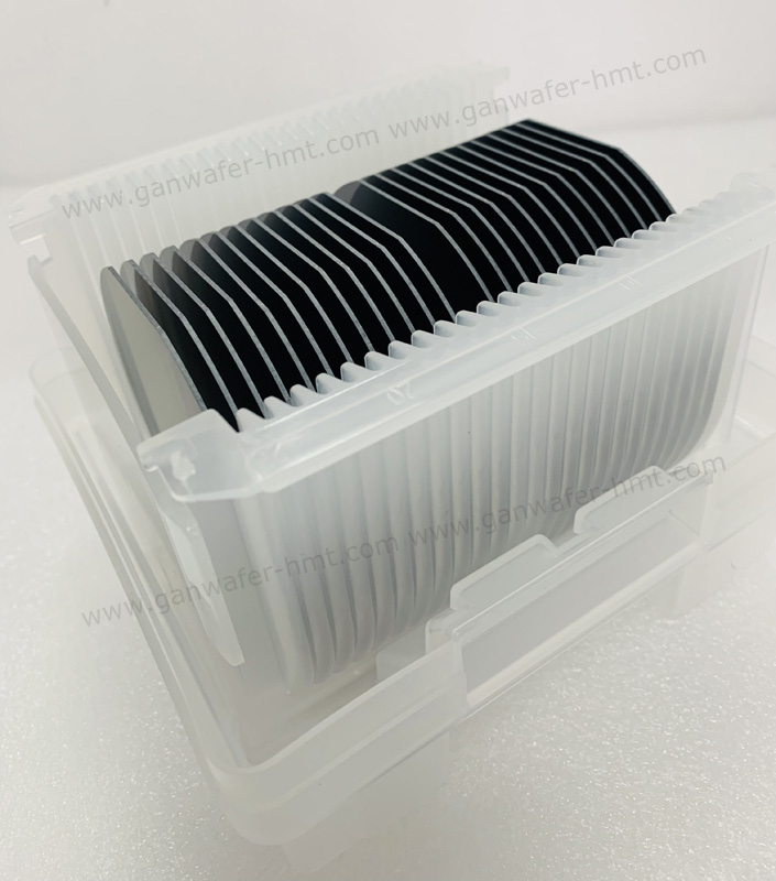
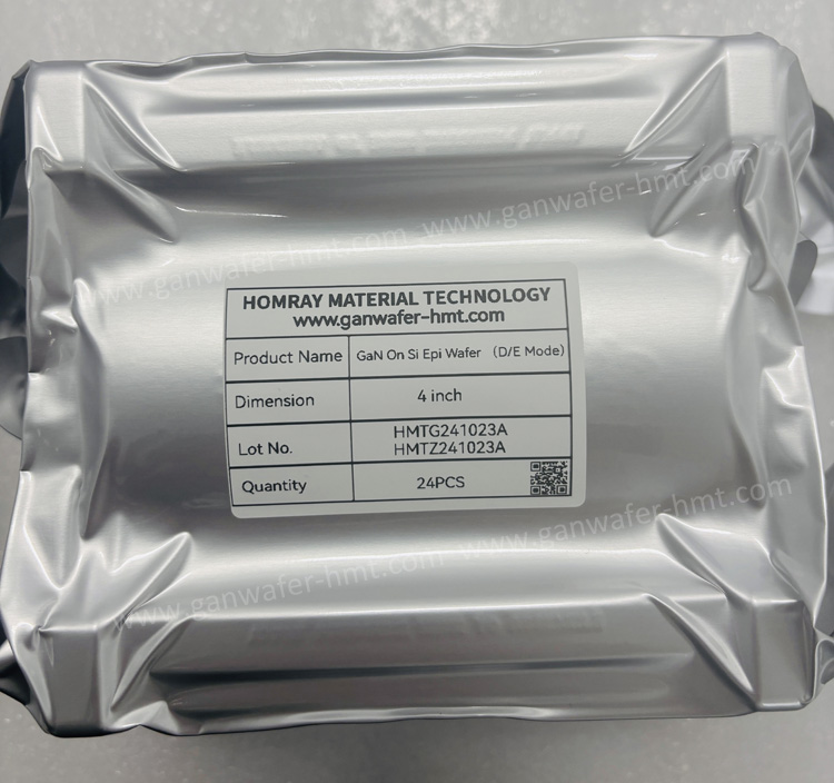
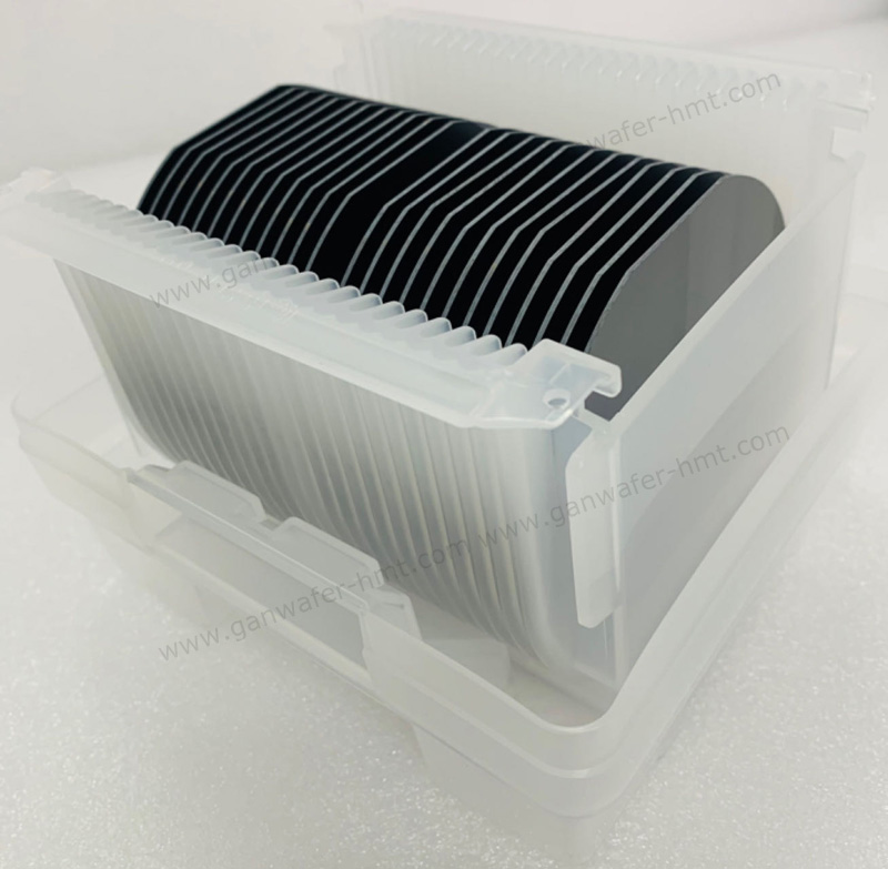
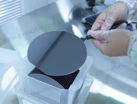
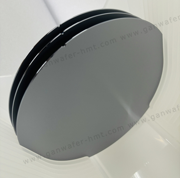
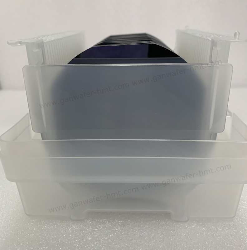
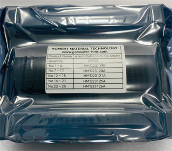
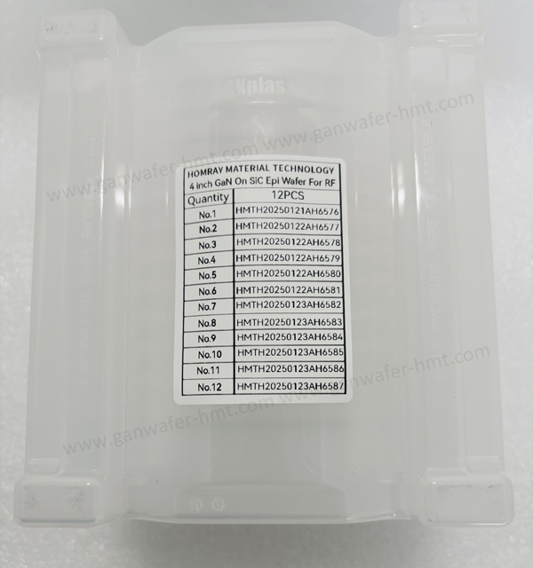
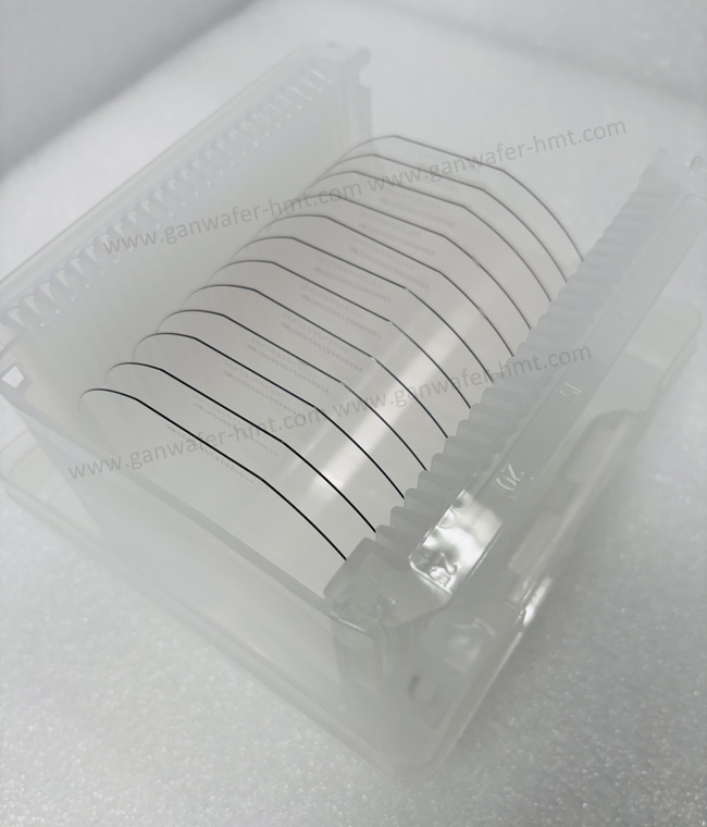
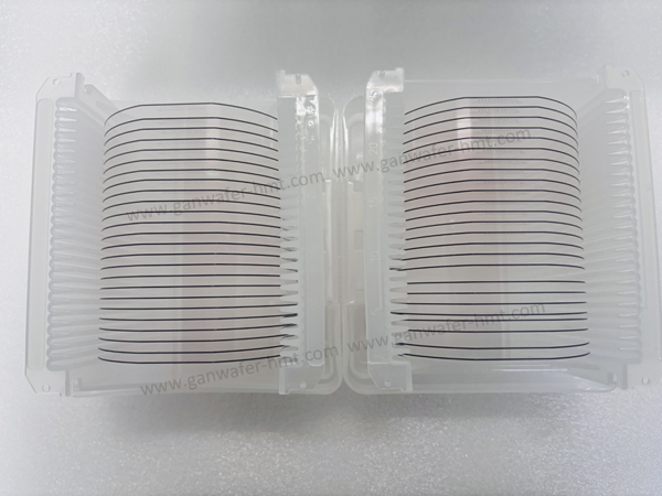
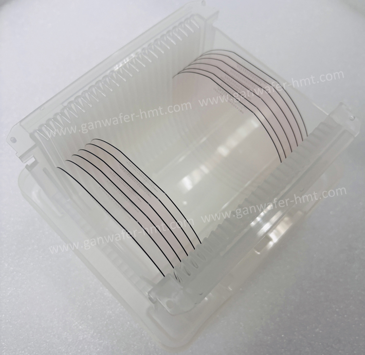
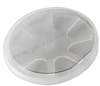
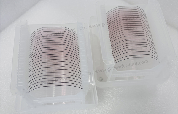
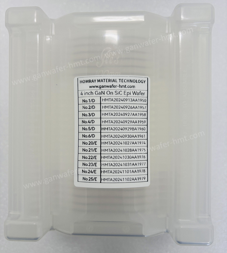
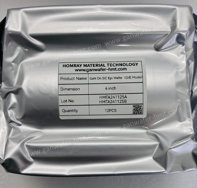
Substrate Size: 4 inch,6 inch
Substrate Thickness: 500um
Type: D-Mode or E-Mode
Product Description
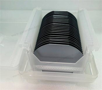
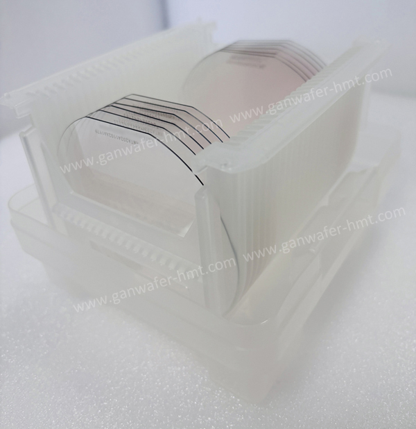
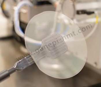
As a professional GaN Epi Wafer manufacturer, we specialize in advanced GaN-on-SiC epitaxial wafer solutions for high-power HEMT applications. Our products includes 4-inch and 6-inch wafers with both D-Mode (depletion-mode) and E-Mode (enhancement-mode) configurations:
-
D-Mode GaN-on-SiC: Available with SiN cap layer or GaN cap layer for optimized high performance and thermal stability.
-
E-Mode GaN-on-SiC: Features a p-GaN cap layer design for enhanced safety and switching efficiency in power electronics.
Based on electrical properties, SiC substrates can be classified into two types:
-
Semi-insulating SiC substrates – Characterized by high resistivity (≥10⁵ Ω·cm), used for high-frequency and high-power RF applications.
-
Conductive SiC substrates – Feature low resistivity (15–30 mΩ·cm), primarily employed in power electronics.
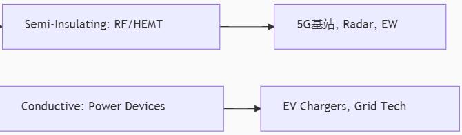
Our GaN-on-SiC epitaxial wafers, grown on semi-insulating SiC substrates, enable the fabrication of high-performance HEMTs (High-Electron-Mobility Transistors) and other microwave/RF devices.
-
-
Meanwhile, We provide fully customizable epitaxial structures, including layer thickness, doping profiles, and stress engineering. Our technical team collaborates closely with clients to:
-
Optimize wafer parameters for specific applications (e.g., 5G基站, radar systems, EV charging).
Related Products
![]() E-mail: kim@homray-material.com;tina@homray-material.com
E-mail: kim@homray-material.com;tina@homray-material.com
HMT Silicon Carbide (SiC) Wafer Website: www.sicwafer-hmt.com