
D-Mode/E-Mode GaN On SiC Epi Wafers
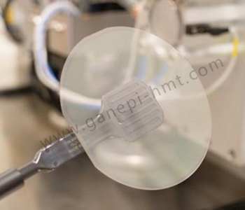
GaN-On-SiC Epi Wafer For Power HEMT
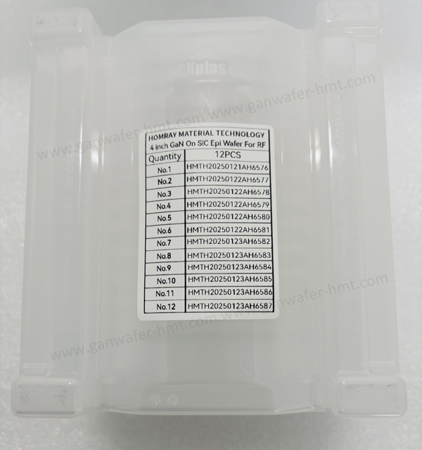
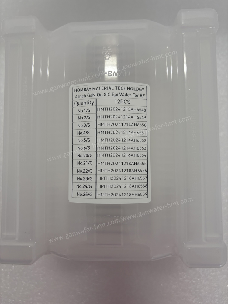
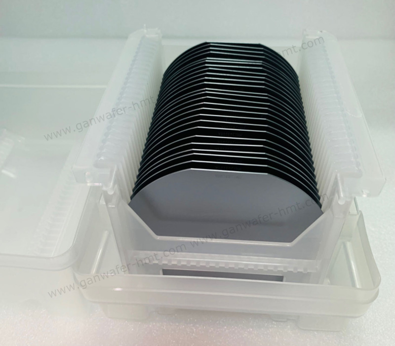
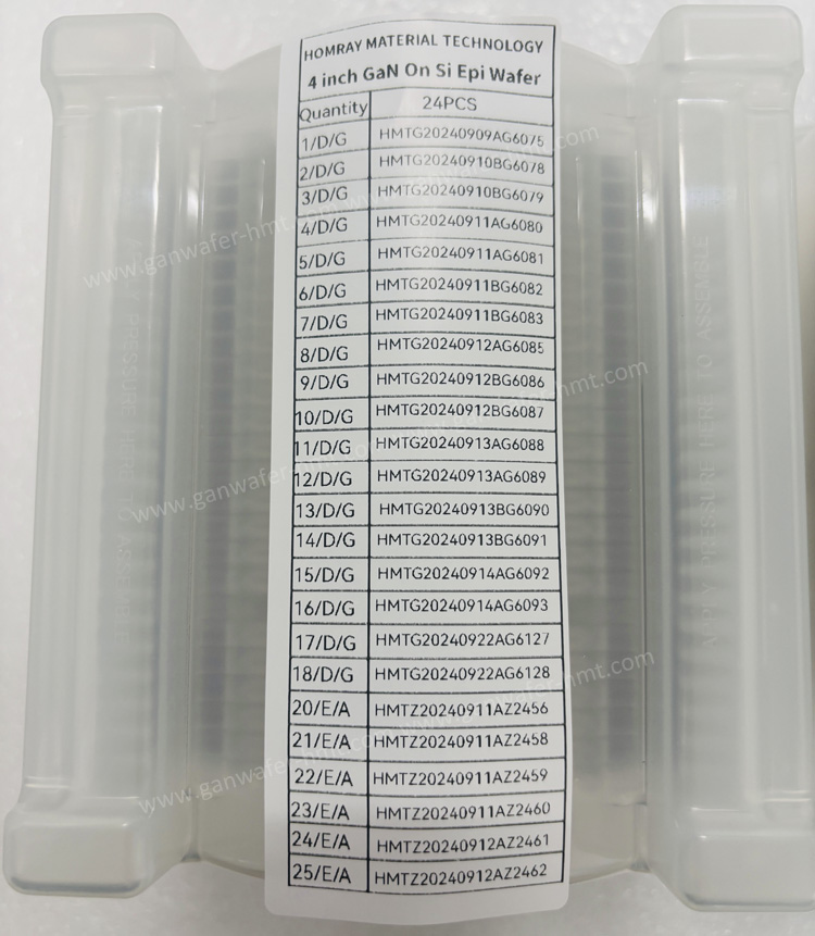
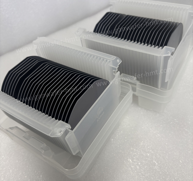
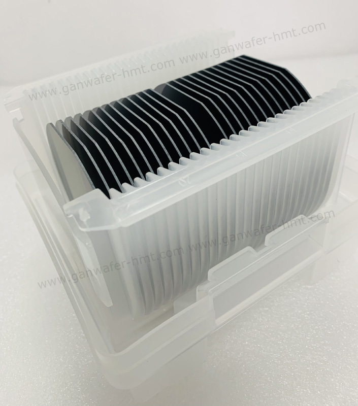
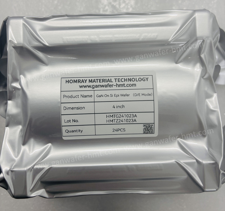
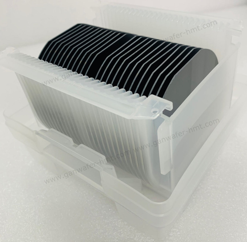
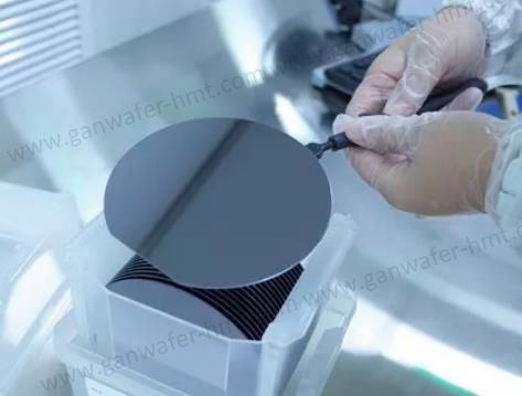
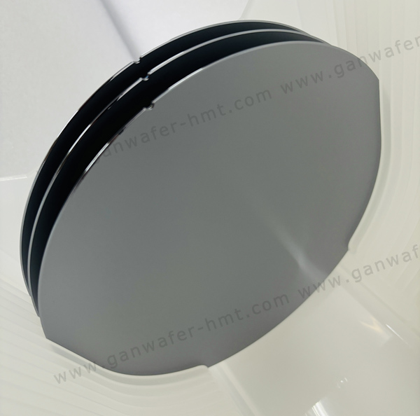
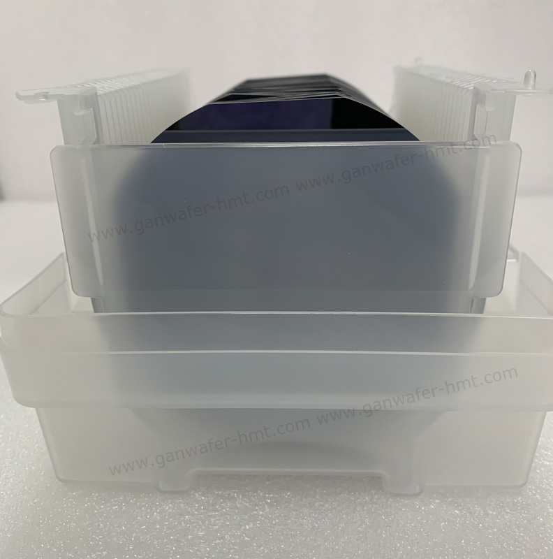
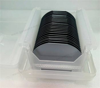
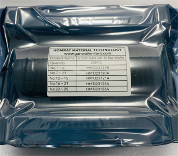
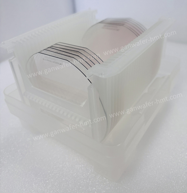
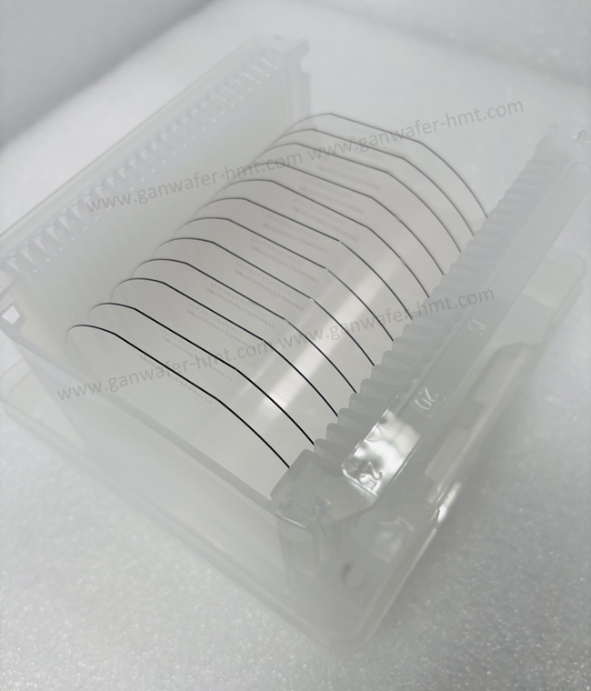
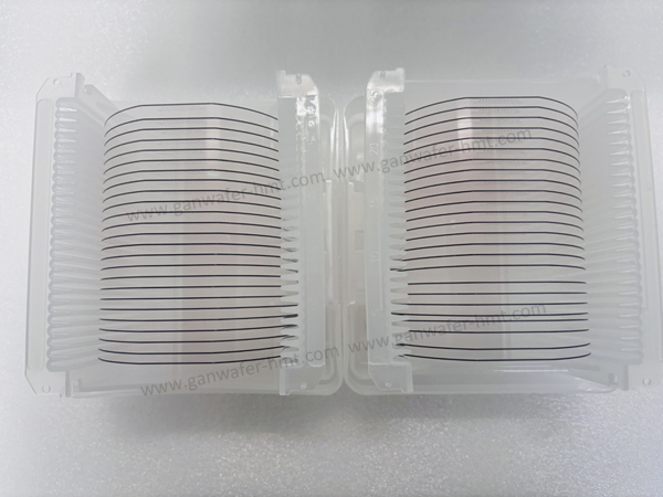
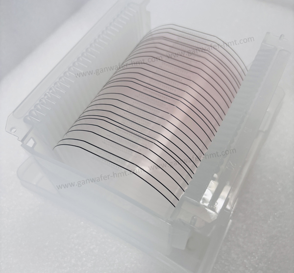
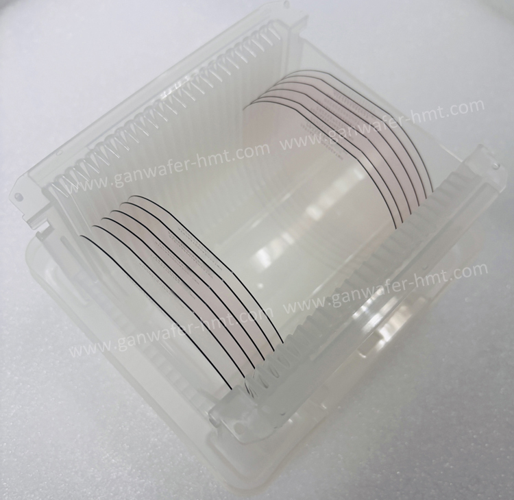
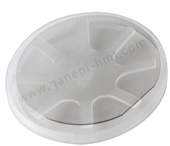
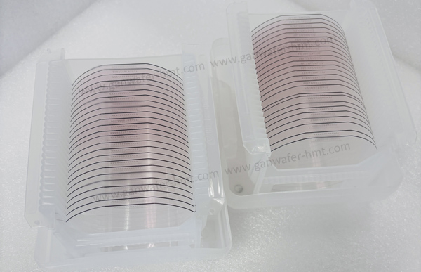
Substrate Size: 4 inch,6 inch
Substrate Thickness: 500um
GaN Cap Layer: 2.5-3.5nm
Product Description
Elevate your high-power and high-frequency designs with our D-Mode and E-Mode GaN on SiC epitaxial wafers. As GaN Epitaxy Wafers Supplier, we providing both 4inch and 6inch For Power HEMT GaN on SiC application. Engineered for superior performance in extreme environments, these wafers combine the high-electron-mobility advantages of Gallium Nitride (GaN) with the unmatched thermal conductivity and breakdown voltage of Silicon Carbide (SiC).

Key Features:
-
Wafer Sizes: 4-inch and 6-inch options for scalability and cost efficiency.
-
Structure Parameters:
-
Cap Layer Thickness: 0-5nm SiN cap or GaN cap for D-Mode and 70-100nm pGaN cap for E-Mode.
-
2DEG Density: >1×10¹³ cm⁻² for ultra-low on-resistance and high current handling.
-
Thermal Conductivity: 390 W/m·K (SiC substrate) for efficient heat dissipation.
-
-
D-Mode/E-Mode Flexibility: Choose between normally-on (D-Mode) or normally-off (E-Mode) configurations to match your circuit design requirements.
Applications:
-
5G & RF Systems: Ideal for high-efficiency RF power amplifiers and mmWave transmitters.
-
Electric Vehicles (EV): Enable fast-charging systems and high-power traction inverters.
-
Defense & Aerospace: Critical for radar, satellite communications, and electronic warfare.
-
Industrial Power: Optimized for renewable energy inverters, UPS, and motor drives.
Why Choose Our GaN Epi Wafers?
-
Reliability: Industry-leading defect density ensures long-term stability.
-
Customization: Tailored doping profiles, buffer layers, and cap layers (e.g., AlGaN) for specific applications.
-
Related Products
![]() M.P: +86-15366208370 ; +86-15366203573
M.P: +86-15366208370 ; +86-15366203573
![]() E-mail: kim@homray-material.com;tina@homray-material.com
E-mail: kim@homray-material.com;tina@homray-material.com
HMT Silicon Carbide (SiC) Wafer Website: www.sicwafer-hmt.com