
Mg Doped p-GaN Epitaxy Wafer Supplier
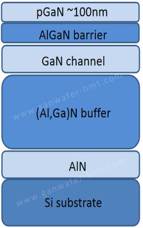
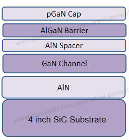
p-GaN on SiC/ p-GaN on Si
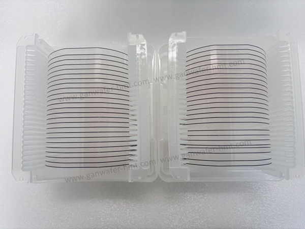
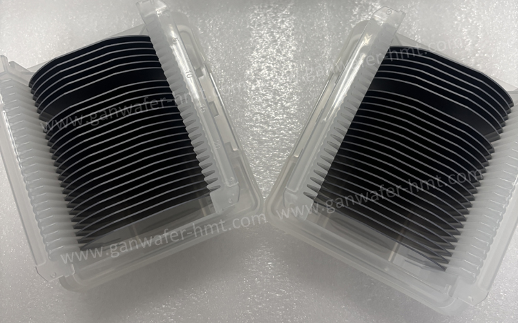
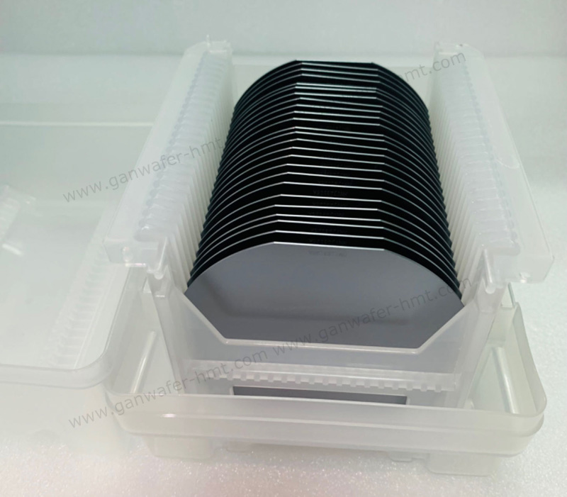
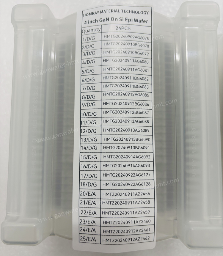
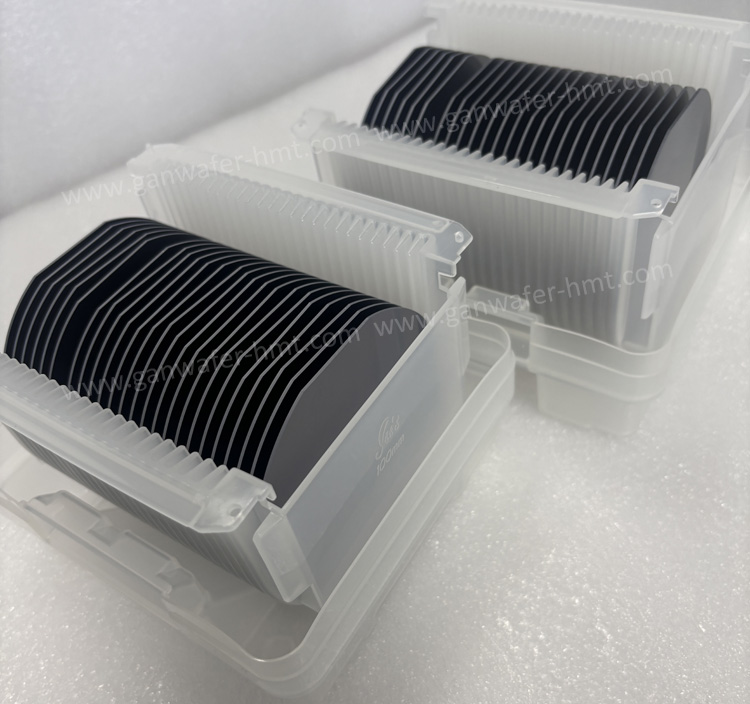
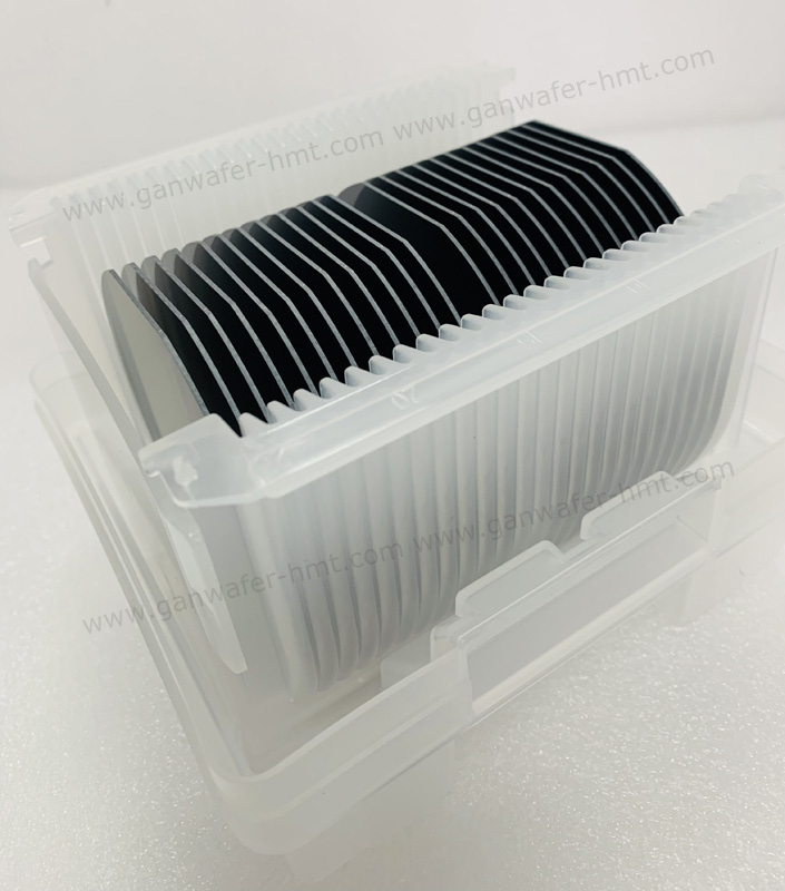
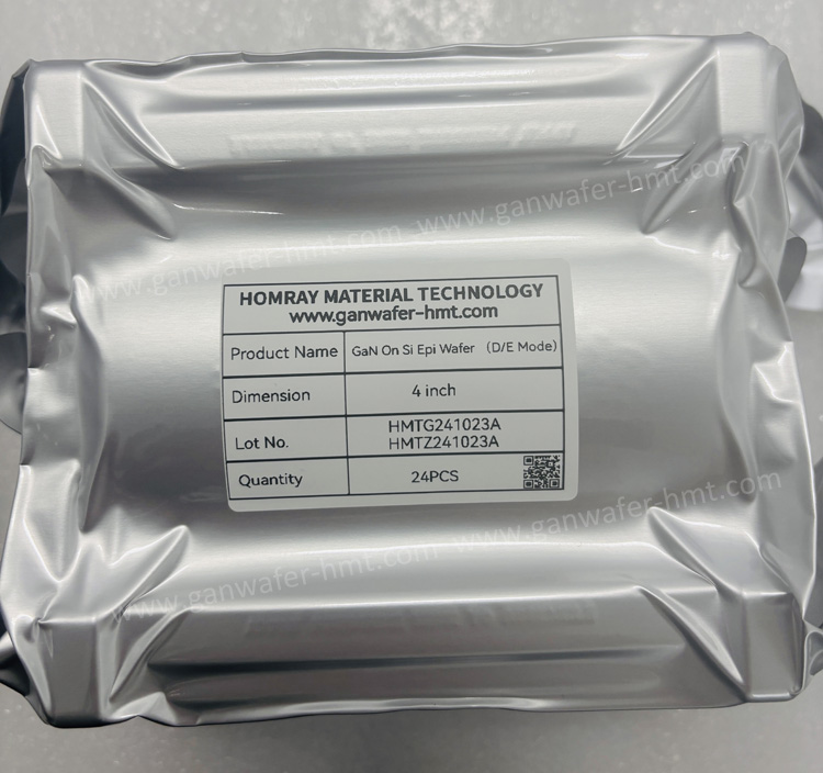
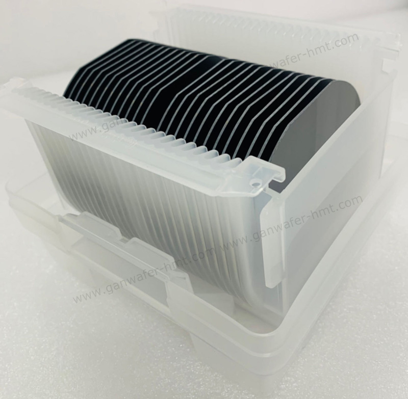
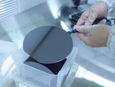
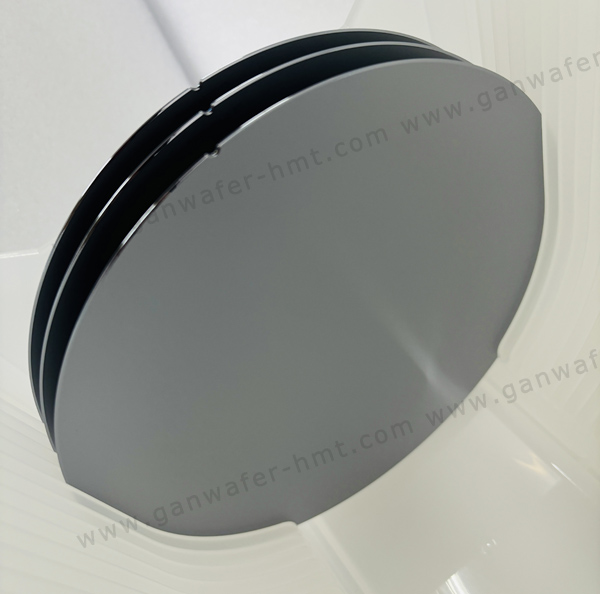
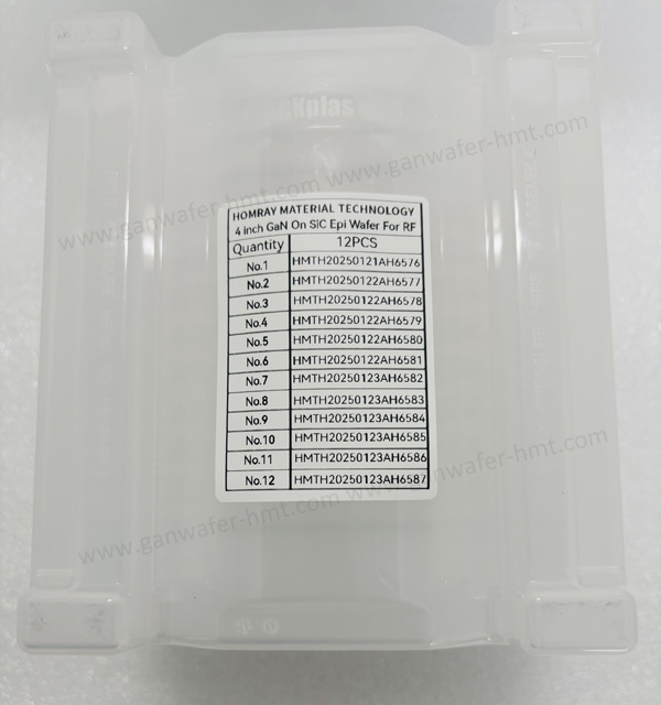
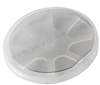
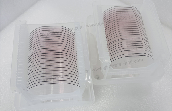
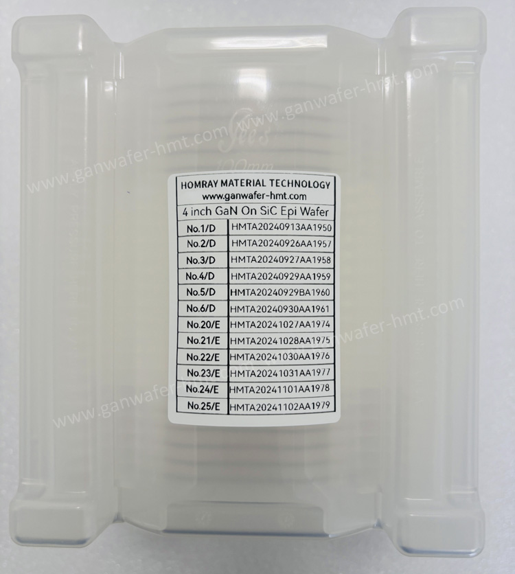
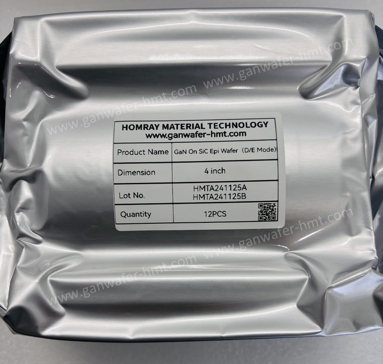
Substrate Size: 4 inch,6 inch,8 inch
Substrate Thickness: 500um/675um
p-GaN Cap Layer: 90-100nm
Product Description
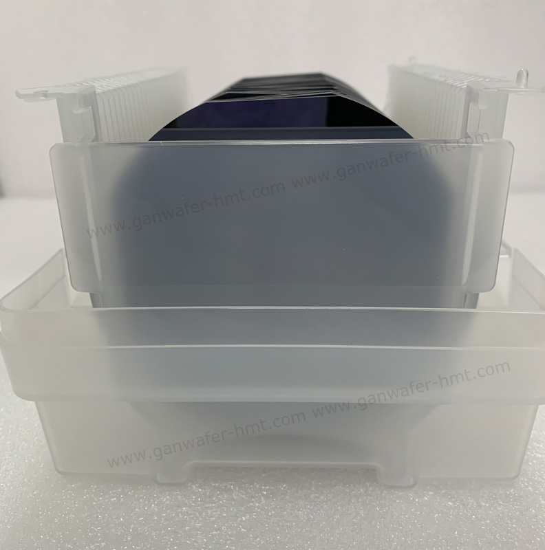
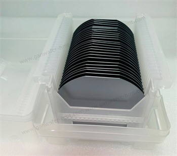
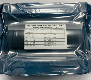
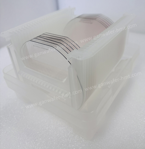
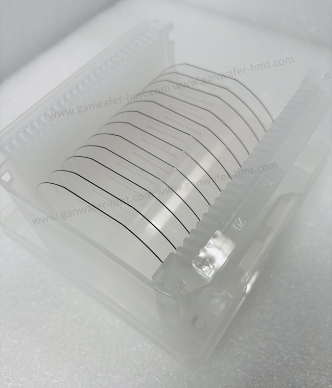
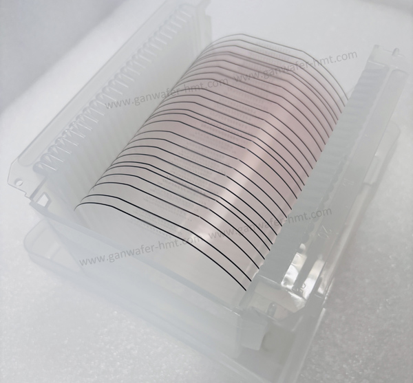
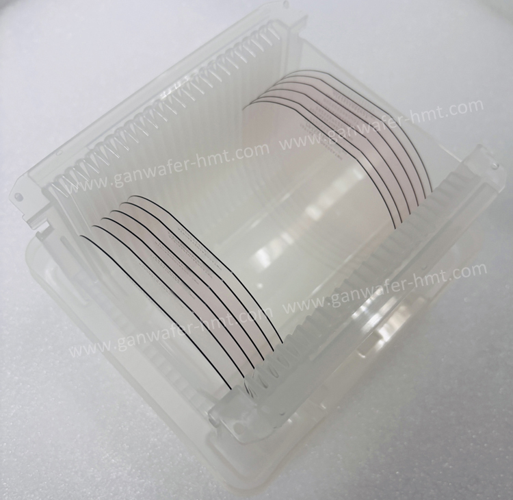
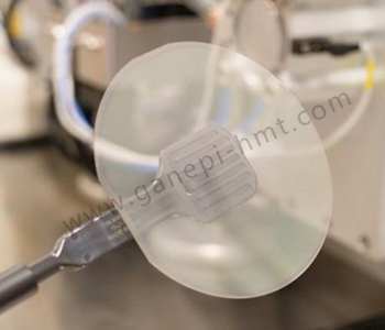
HMT company produces p-GaN on SiC and p-GaN on Si Epi Wafer to worldwide semiconductor companies and research labs. We supply 4'' 6'' and 8'' pGaN Epi Wafers and support customization.
The enhanced-mode p-GaN gate HEMT achieves intrinsic normally-off operation by incorporating a p-type GaN layer in the gate region of the AlGaN/GaN heterostructure. This design enables complete device turn-off at zero to negative bias, making it an ideal solution for high-voltage, high-power applications.
Compared to conventional D-mode devices, the E-mode p-GaN HEMT demonstrates superior performance in:
-
Threshold gate voltage characteristics
-
Switching performance
-
Operational reliability
Furthermore, its MOSFET-like driving mechanism significantly simplifies system design requirements.
With the GaN device market rapidly expanding, enhanced-mode p-GaN HEMTs are becoming the technology of choice for:
-
Electric vehicles (EVs)
-
Solar inverters
-
Data center power systems
-
5G base station RF frontends
Emerging dielectric and ferroelectric layers are expected to further enhance threshold voltage control and reliability, unlocking new innovations in GaN power devices.
Related Products
![]() E-mail: kim@homray-material.com;tina@homray-material.com
E-mail: kim@homray-material.com;tina@homray-material.com
HMT Silicon Carbide (SiC) Wafer Website: www.sicwafer-hmt.com