
Power HEMT GaN On SiC Epi Wafer Manufacturer
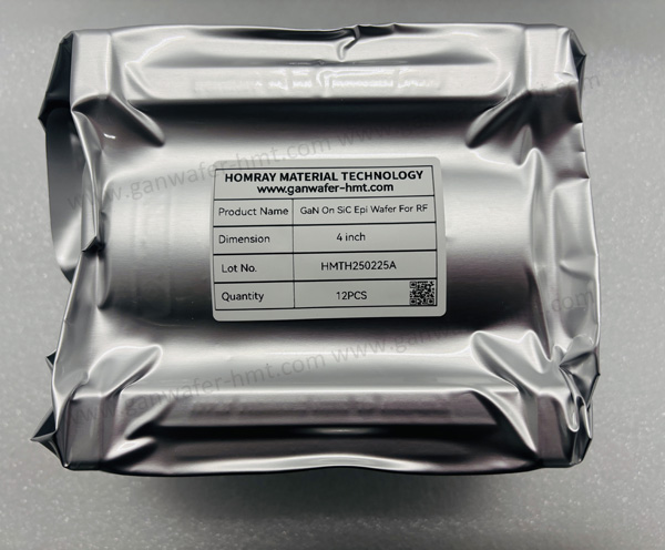
GaN-On-SiC Epi Wafer For Power HEMT
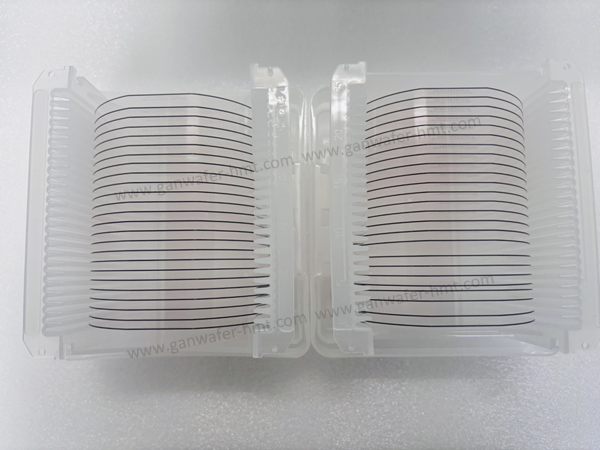
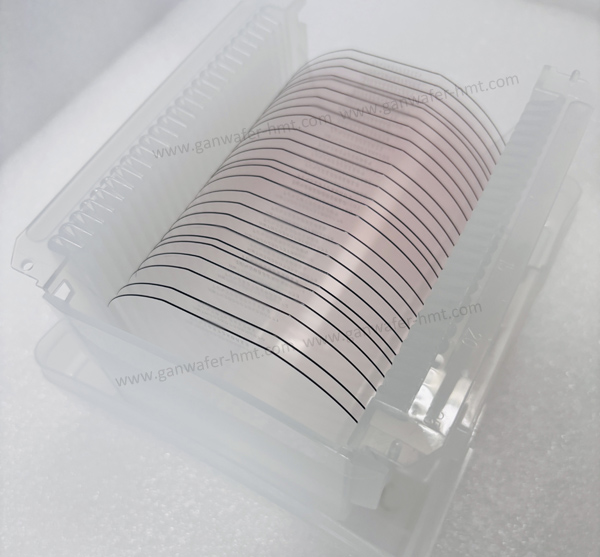
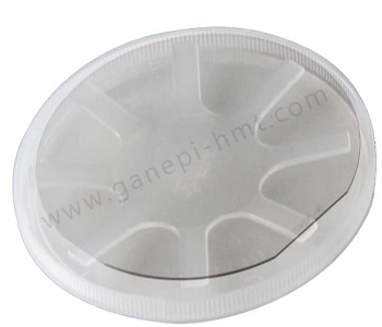
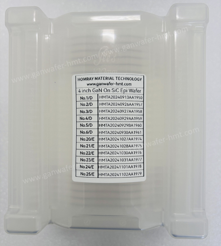
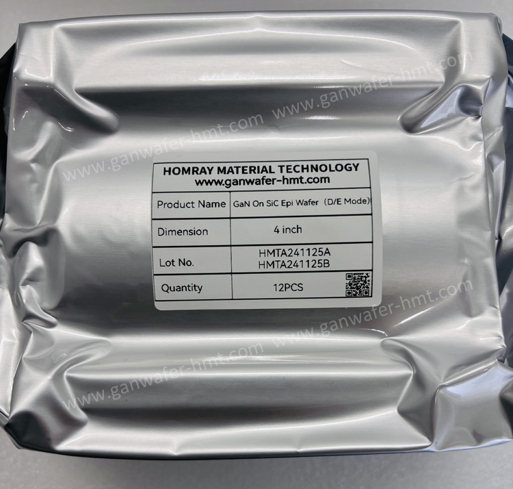
Substrate Size: 4 inch,6 inch
Substrate Thickness: 500um
Cap Layer: GaN or SiN
Product Description
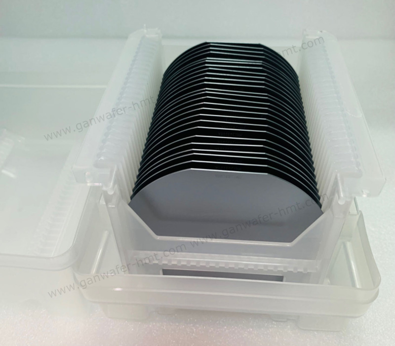
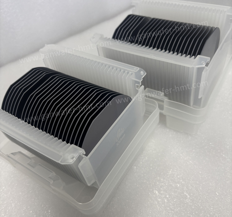
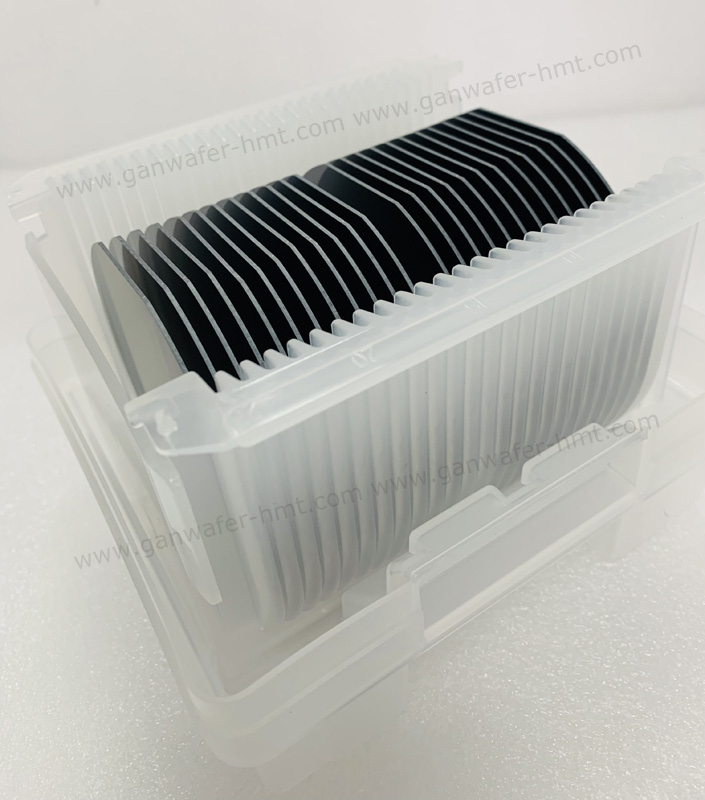
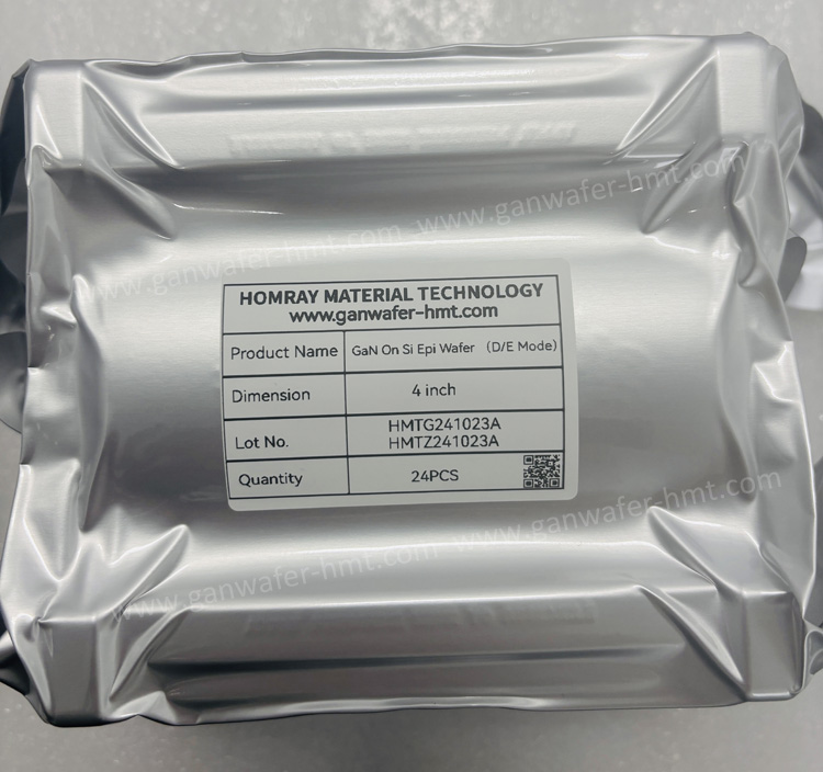
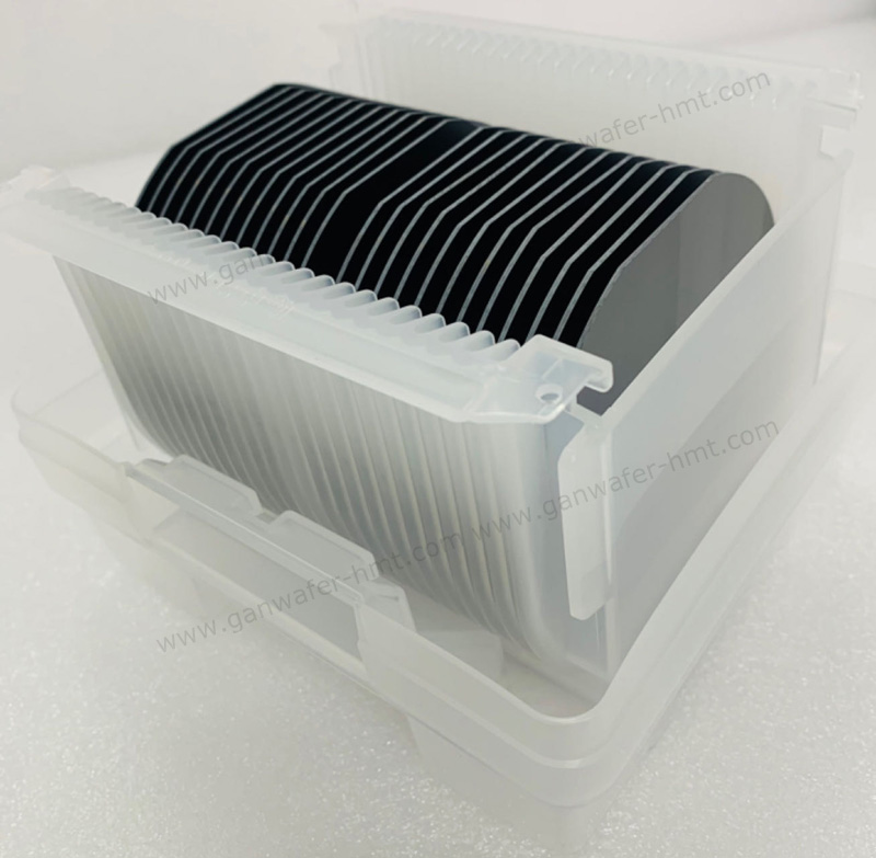
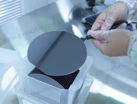
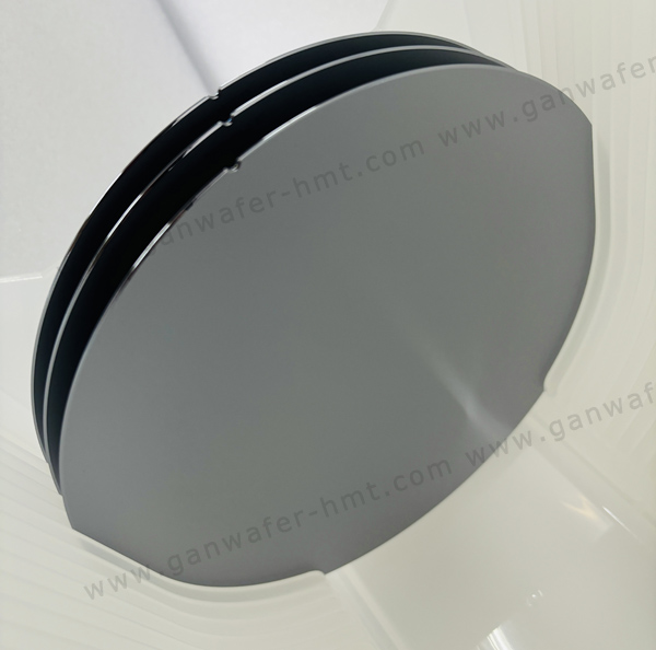
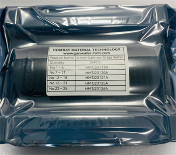
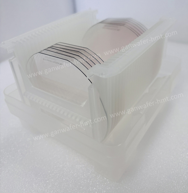
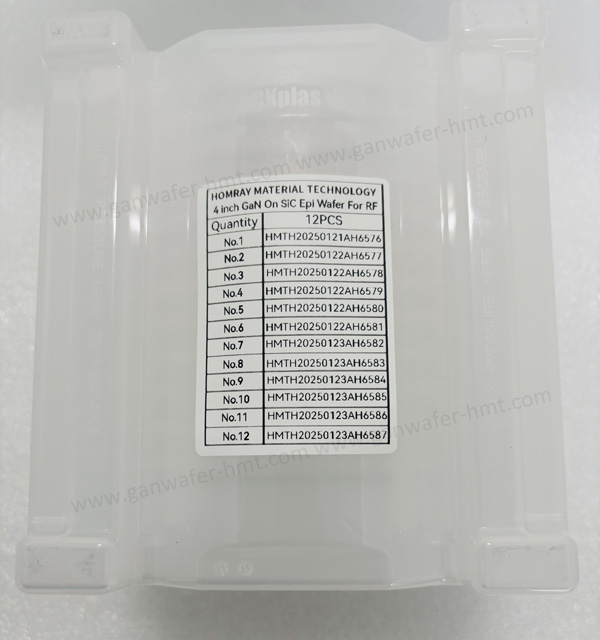
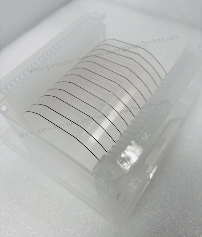
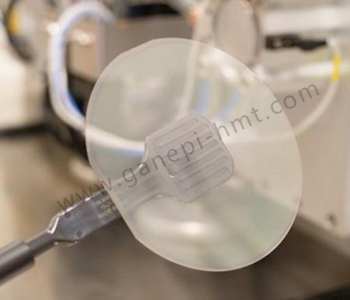
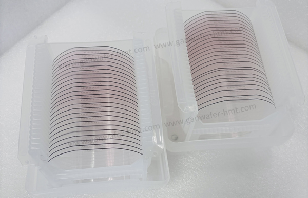
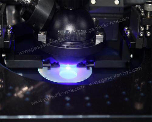
HMT offers high - quality Gallium Nitride (GaN) epitaxial wafers grown on 100mm or 150mm silicon carbide (SiC) substrates.These GaN on SiC Epi wafers are the result of advanced manufacturing processes and strict quality control. The use of SiC substrates provides excellent thermal conductivity, which is crucial for high - power and high - frequency applications. This feature effectively dissipates heat, enhancing the stability and reliability of the device.
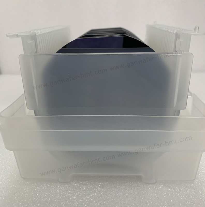
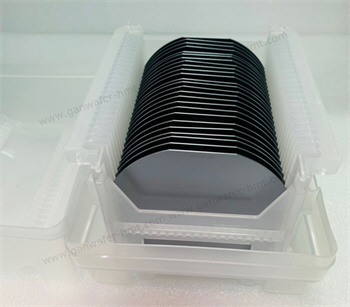
 With a 100mm or 150mm size, our GaN epitaxial wafers are well - suited for large - scale production, enabling higher production efficiency and lower costs. The high - quality GaN on SiC epi wafers have superior electron mobility and breakdown voltage, which is ideal for manufacturing high - performance semiconductor devices such as 5G communication base - station power amplifiers, high - power LED lighting, and electric vehicle power modules.
Key Specifications
-
Substrate Options: 100mm & 150mm SiC wafers (N-Type & Semi-Insulating)
-
Crystal Quality: <5E7 cm⁻² dislocation density with <30μm wafer bow
-
Custom Sizes: 4-inch and 6-inch configurations (AlGaN/GaN heterostructures)
Application-Specific Solutions-
5G mmWave: 64QAM Massive MIMO amplifiers (24-40GHz)
-
Satellite Comms: Radiation-hardened LNA/PA modules for LEO constellations
-
Defense Systems: X-band radar FEMs with 100kW+ peak power handling
-
EV Fast Charging: 1.2kV HEMTs enabling 350kW ultra-fast DC stations
-
Whether you are looking to develop cutting - edge communication technologies or high - power electronic products, our 100mm or 150mm SiC - based GaN epitaxial wafers are your reliable choice.
Related Products
![]() M.P: +86-15366208370 ; +86-15366203573
M.P: +86-15366208370 ; +86-15366203573
![]() E-mail: kim@homray-material.com;tina@homray-material.com
E-mail: kim@homray-material.com;tina@homray-material.com
HMT Silicon Carbide (SiC) Wafer Website: www.sicwafer-hmt.com