
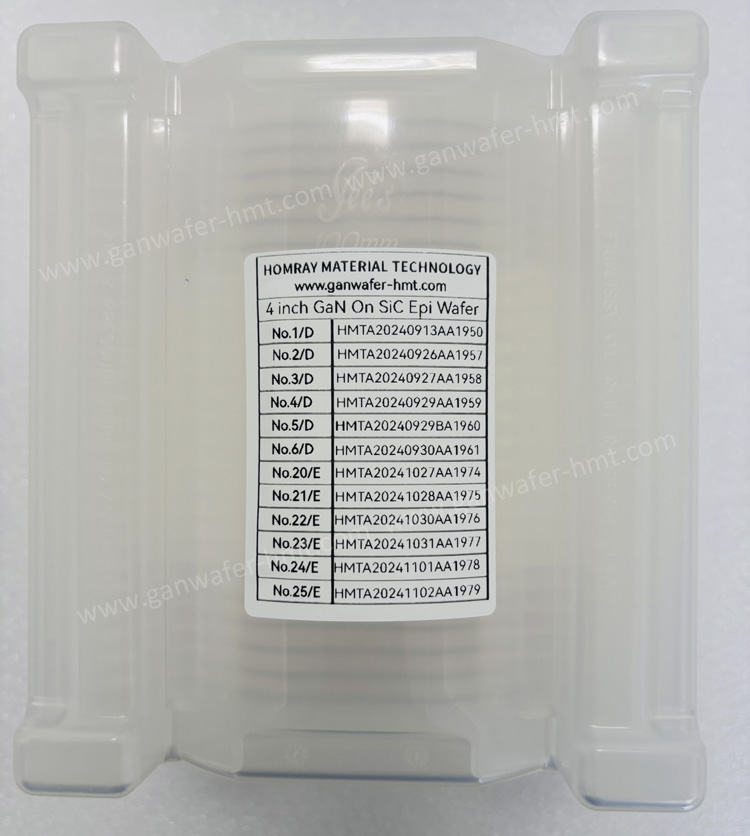

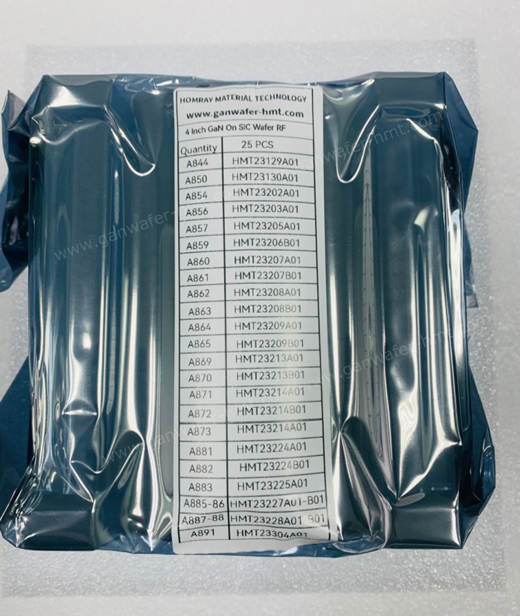
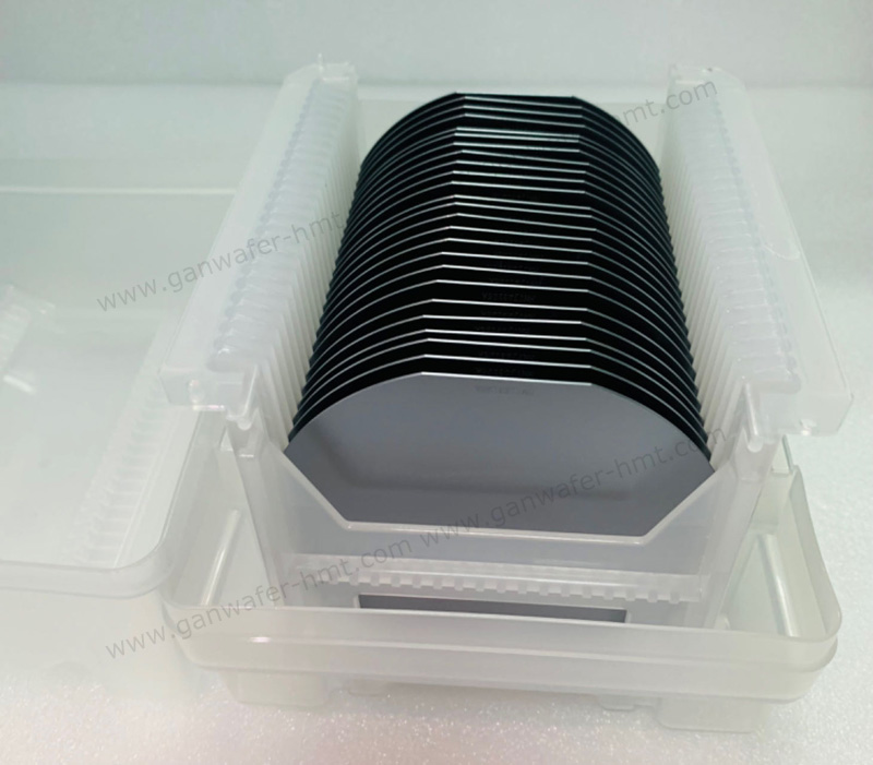
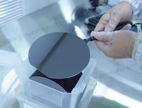
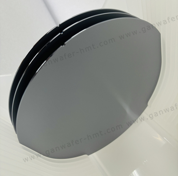
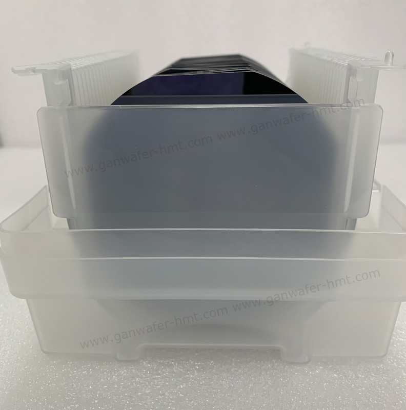
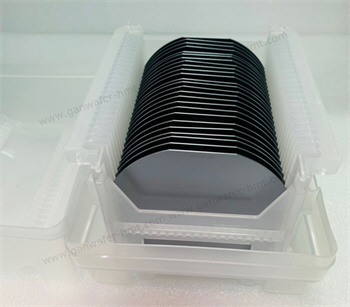
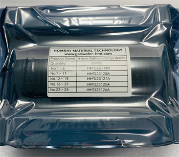
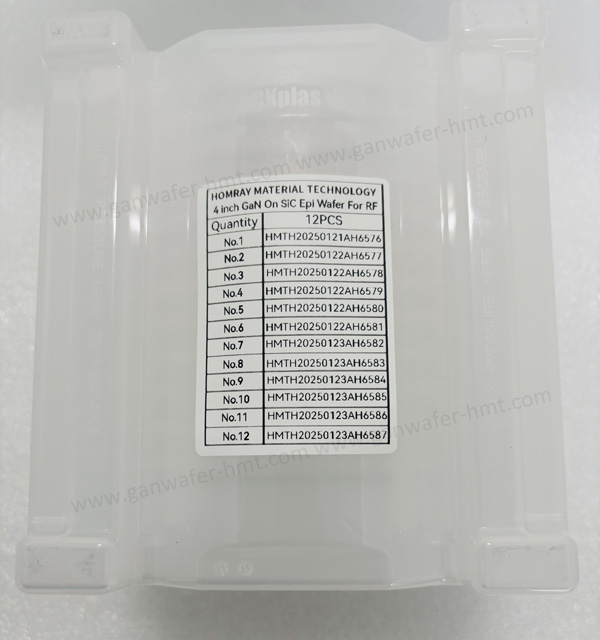
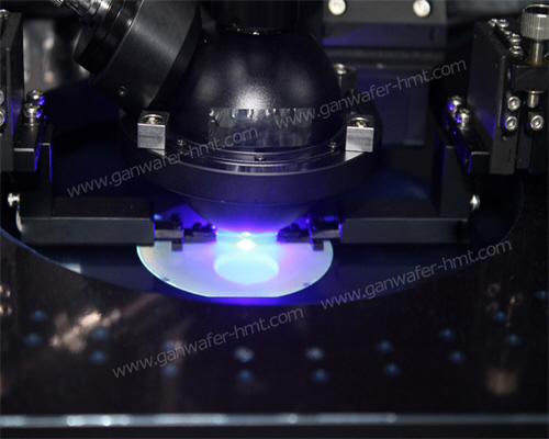
4 Inch RF HEMT GaN-On-SiC Epi Wafer Manufacturer
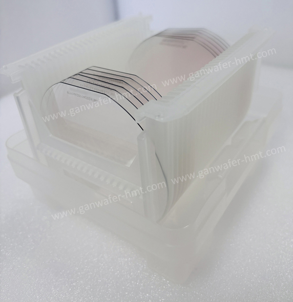
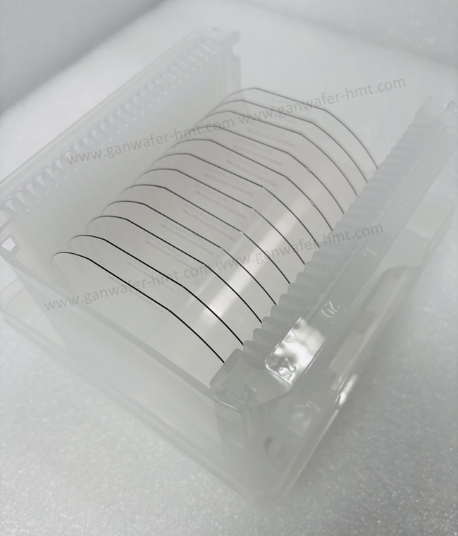
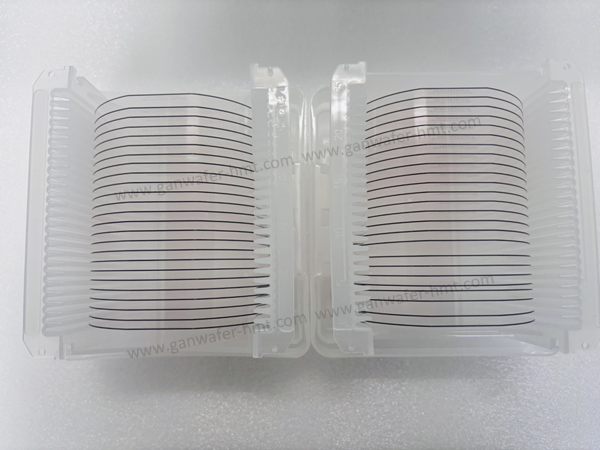
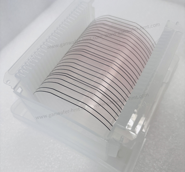
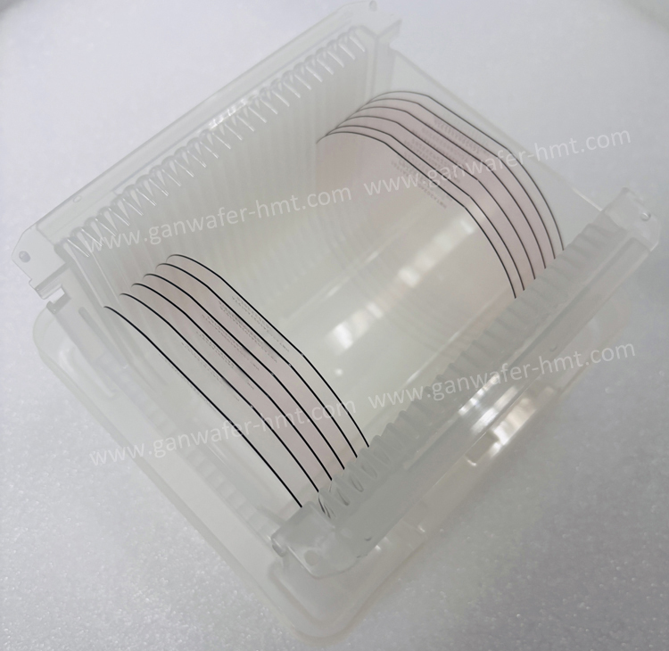
GaN-On-SiC Epi Wafer
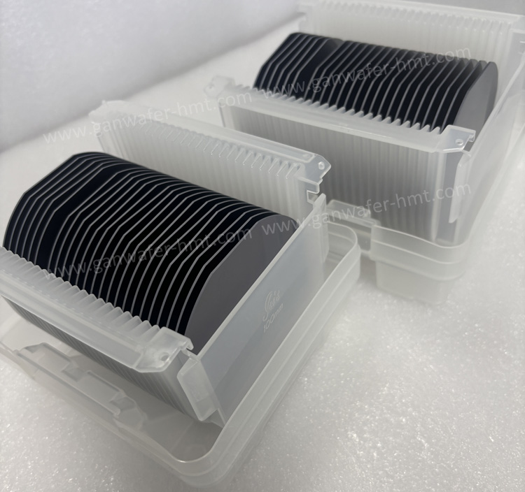
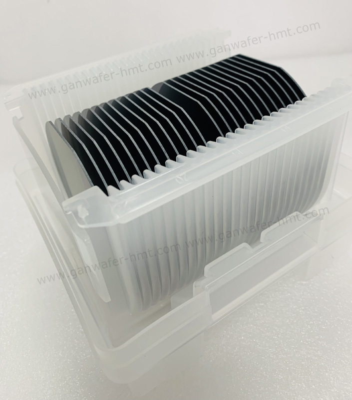
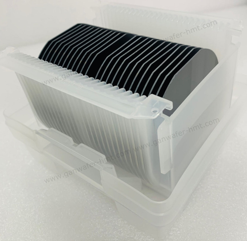
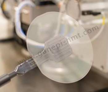
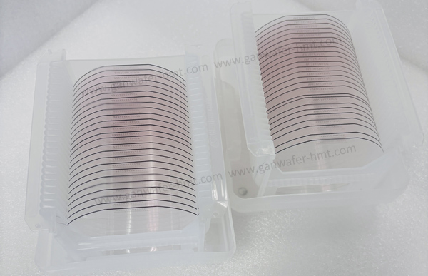
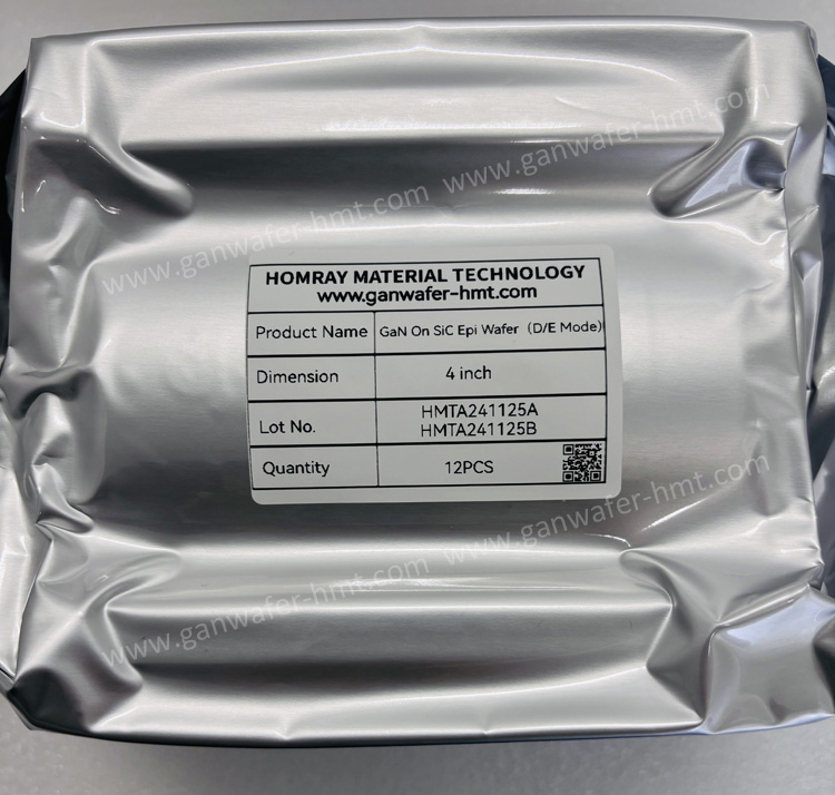
Substrate Size: 4 inch,6 inch
Substrate Thickness: 500um
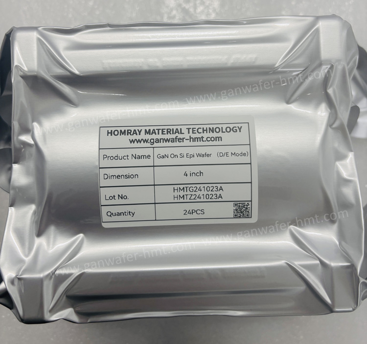
Package: Wafer Cassette
Product Description
Buy GaN-on-SiC epi wafer manufacturer and supplier from HMT China, 4 inch and 6 inch GaN/SiC RF HMET structure for microwave electronic devices. We use high qulity 4H-SI SiC substrate, thickness 500um. The thickness of GaN buffer layer is 1.8um, and the spacer layer of aluminum nitride is 1nm.With our rich experience and knowledge in the GaN epi wafer industry, customers can be confident cooperate with us.
Benefits of using GaN
High power
High frequency
High power efficiency
Low power consumption, energy saving
High-temperature robustness
Exceed the limitations of current Si power device
Technical application of GaN in electric vehicles
Back in 2020, an all-gallium nitride car with solar cells, demonstrating the feasibility of gallium nitride in power conversion and proving that gallium nitride also has great application prospects in automobiles. For example, the AS1531 on-board charger (OBC) for electric vehicles, using GaN devices, can reduce the size to one-fifth of the original, the charging efficiency can reach 98%, and the heat dissipation structure can also be reduced. The significant improvement of GaN devices on DC/DC is that the power density is greatly improved, which can be increased from 1kw/L to 2kw/L.

Related Products
![]() E-mail: kim@homray-material.com;tina@homray-material.com
E-mail: kim@homray-material.com;tina@homray-material.com
HMT Silicon Carbide (SiC) Wafer Website: www.sicwafer-hmt.com